

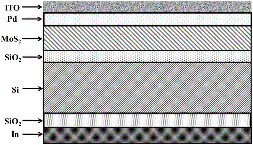
MoS2/Si photovoltaic device with ITO/Pd double-layer structured composite electrode and preparation method thereof
A composite electrode, double-layer structure technology, used in photovoltaic power generation, electrical components, semiconductor devices, etc., can solve the deterioration of metal layer continuity, reduce the collection efficiency of photo-excited carriers, reduce the short-circuit current density of the device and the light conversion efficiency. and other photovoltaic performance issues, to achieve the effects of reducing absorption, improving sunlight transmittance, reducing open circuit voltage and light conversion efficiency
- Summary
- Abstract
- Description
- Claims
- Application Information
AI Technical Summary
Problems solved by technology
Method used
Image

Examples
Embodiment 1
[0077] The preparation method is as follows:
[0078] The first step, silicon substrate surface passivation step
[0079] Select a p-type Si single crystal substrate with a resistivity of 1-2 Ω cm and a crystal plane orientation of (100) plane, and ultrasonically clean it in alcohol, acetone and deionized water for 180 s in sequence;
[0080] Take out the cleaned Si substrate and dry it with nitrogen;
[0081] Then, put the dried Si single crystal substrate into a beaker filled with a hydrogen peroxide solution with a volume fraction of 30%, place the beaker in a water bath, and heat it in a water bath at 100°C for 10 minutes to perform surface passivation. change;
[0082] Take it out, wash it in deionized water for one minute; take it out and dry it with high-purity nitrogen, that is, the surface passivation of the Si single crystal substrate is completed, and the upper and lower surfaces have SiO 2 Si substrate of passivation layer;
[0083] The second step, MoS 2 Thin...
Embodiment 2
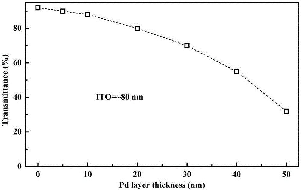
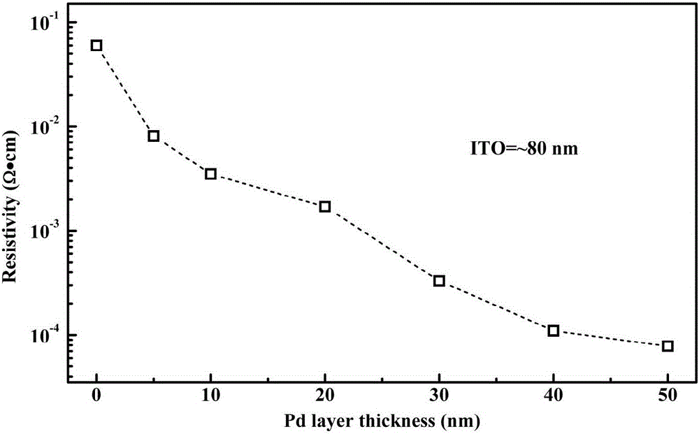
[0096] Explanation: This example is a comparative example, the front electrode of the device only has a Pd metal layer, and there is no ITO conductive transparent oxide layer.
[0097] The first step to the third step are all the same as in Example 1.
[0098] The fourth step is the preparation step of the In back electrode, the method is as follows:
[0099] Take out the surface deposited with Pd / MoS 2 The Si single crystal substrate of the multilayer thin film is welded to the SiO on the lower surface of the Si substrate by soldering. 2 On the passivation layer, an In back electrode is formed.
[0100] Product performance test results:
[0101] After testing, at 30mWcm -2 Under white light conditions, the prepared MoS 2 / Si heterojunction photovoltaic solar cell device with a photoexcited current density of 5.5 mAcm -2 , open circuit voltage 0.35V, conversion efficiency 2.2%.
Embodiment 3
[0103] Explanation: This example is a comparative example. The front electrode of the device only has an ITO transparent conductive layer, and the ITO transparent conductive layer is directly sputtered and deposited on MoS 2 on the surface of the film layer. That is, there is no Pd metal layer.
[0104] The first step and the second step are all the same as in Example 1.
[0105] The third step is the surface deposition step of the ITO transparent conductive layer, the method is as follows:
[0106] Replace the tray with the sample directly above the ITO target;
[0107] Adjust the temperature of the Si single crystal substrate to the third temperature of 80°C, adjust the argon gas pressure to the third pressure of 0.5Pa, adopt DC magnetron sputtering technology, and use the ionized ions under the condition of constant 30W sputtering power Bombarding the ITO target, depositing an ITO conductive transparent oxide layer with a thickness of 80nm on the surface of the above-men...
PUM
| Property | Measurement | Unit |
|---|---|---|
| Resistivity | aaaaa | aaaaa |
| Thickness | aaaaa | aaaaa |
| Thickness | aaaaa | aaaaa |
Abstract
Description
Claims
Application Information