Method for located growing of big single crystal graphene on SiC substrate through point-seed way

A single crystal graphene, large-size technology, applied in the field of microelectronic materials, can solve the problems of uncontrollable single nucleation, difficulty in obtaining large-size single crystal graphene, and unavoidable damage and pollution of graphene

Active Publication Date: 2017-03-22
山东本源晶体科技有限公司
View PDF13 Cites 3 Cited by
  • Summary
  • Abstract
  • Description
  • Claims
  • Application Information

AI Technical Summary

Problems solved by technology

Although adopting this method can obtain large crystal domains of graphene, the same as patent document CN103074878A and patent document CN104498902A, the damage and pollution problems caused by graphene in the transfer process cannot be avoided
[0009] Chinese patent document CN103204498A discloses a method for preparing epitaxial graphene by thermally cracking silicon carbide. The process of preparing epitaxial graphene by thermally cracking silicon carbide under the assistance of argon gas is improved on

Method used


Image

  • Method for located growing of big single crystal graphene on SiC substrate through point-seed way
  • Method for located growing of big single crystal graphene on SiC substrate through point-seed way
  • Method for located growing of big single crystal graphene on SiC substrate through point-seed way

Examples


Embodiment 1

[0046] A method for growing large-area graphene by point seed crystal positioning on SiC, comprising the following steps:

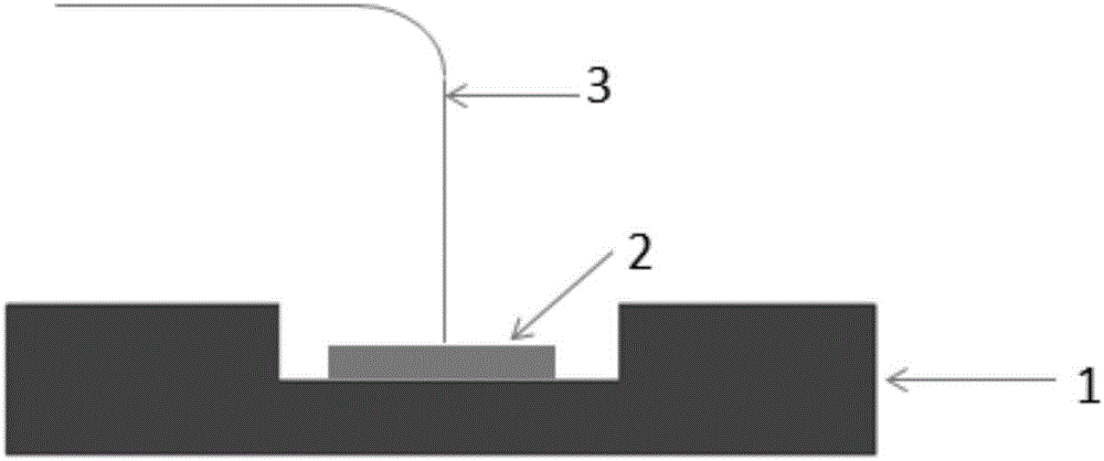
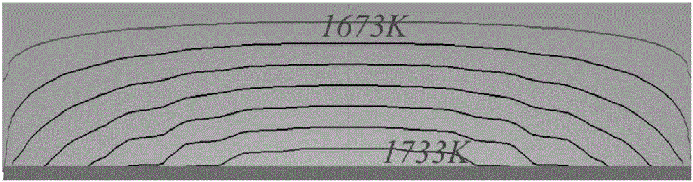
[0047] (1) After the SiC is polished and cleaned, it is placed flat in the heater in the high-temperature CVD graphene growth furnace, and the vacuum degree of the furnace chamber is 10 -3 Pa, the temperature is raised rapidly to 1200°C, and the heating rate is 10°C / min; high-purity argon and hydrogen are introduced, the flow rates are 40sccm and 40sccm, respectively, and the pressure is controlled at 800mbar, and then the temperature is slowly raised to 1500°C, and the heating rate is 2°C / min min, keep it warm for 10 minutes, and carry out hydrogen etching; after the etching, turn off the hydrogen, continue to flow argon, and then slowly lower the temperature to 1400°C, reaching the temperature at which the Si-C bond begins to break. The bond is partially broken and part of the silicon evaporates. The surface topography of the SiC atomic force microscop...

Embodiment 2

[0052] A method for growing large-area graphene by point seed crystal positioning on SiC, comprising the following steps:

[0053] (1) After the SiC is polished and cleaned, it is placed flat in the heater in the high-temperature CVD graphene growth furnace, and the vacuum degree of the furnace chamber is 10 -3 Pa, heat up to 1300°C quickly, with a heating rate of 10°C / min; feed high-purity argon and hydrogen with flow rates of 50sccm and 50sccm respectively, and control the pressure at 900mbar, then slowly raise the temperature to 1500°C, with a heating rate of 2°C / min min, keep it warm for 10 minutes, and carry out hydrogen etching; after the etching, turn off the hydrogen, continue to flow argon, and then slowly lower the temperature to 1400°C, reaching the temperature at which the Si-C bond begins to break. The bond is partially broken and part of the silicon evaporates.

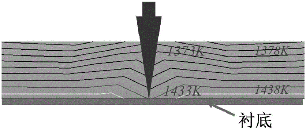
[0054] Then, the temperature was lowered to 1000°C in an argon atmosphere, and the platinum micro-th...

Embodiment 3

[0059] A method for growing large-area graphene at SiC using point seed orientation, comprising steps as follows:

[0060] (1) After the SiC is polished and cleaned, it is placed flat in the heater in the high-temperature CVD graphene growth furnace, and the vacuum degree of the furnace chamber is 10 -4 Pa, heat up to 1200°C quickly, with a heating rate of 10°C / min; feed high-purity argon and hydrogen, with flow rates of 50sccm and 40sccm, respectively, and control the pressure at 850mbar, then slowly raise the temperature to 1600°C, with a heating rate of 5°C / min min, keep it warm for 10 minutes, and carry out hydrogen etching; after the etching, turn off the hydrogen, continue to flow argon, and then slowly lower the temperature to 1400°C, reaching the temperature at which the Si-C bond begins to break. The bond is partially broken and part of the silicon evaporates.

[0061] Then, the temperature was lowered to 1100 °C in an argon atmosphere, and the platinum micro-thermal...


PUM


Abstract

The invention relates to a method for located growing of big single crystal graphene on a SiC substrate through a point-seed way. The method comprises the following steps: (1) polishing and cleaning SiC; feeding into a growing furnace; pumping vacuum; increasing the temperature to be 1200 to 1300 DEG C; charging argon and hydrogen; increasing the temperature to be 1500-1600 DEG C; performing hydrogen etching; closing hydrogen after etching; decreasing the temperature to be 1400 to 1500 DEG C, and maintaining the temperature; decreasing the temperature to be 800 to 1100 DEG C under argon atmosphere; placing a superfine heat conducting probe on the SiC substrate to form a local undercooling point; charging carbon source gas and hydrogen, wherein an active carbon source obtained by the decomposing of the carbon source gas can preferentially grow into graphene seed crystal at the undercooling point; (2) enabling continuous growing of graphene using the seed crystal on the SiC substrate as the center under the condition that the temperature is 800 to 1100 DEG C, the pressure is 800 to 900mbar, and carbon source gas is supplied, so as to obtain big single crystal graphene; and (3) charging argon after the growth, and decreasing the temperature, thus obtaining the big single crystal graphene. The method is free of a metal substrate, and the grown big single crystal graphene can be directly applied to micro-electronic appliance without being transferred.

Description

technical field [0001] The invention relates to a new method for positioning and growing large-size single crystal graphene on a SiC substrate through a point seed crystal process, and belongs to the technical field of microelectronic materials. Background technique [0002] Graphene is composed of C atoms with sp 2 The hexagons composed of orbitals form a honeycomb-like monolayer of atomic two-dimensional crystals. In 2004, the team of Geim and Novoselov at the University of Manchester in the United Kingdom first used tape micromechanical exfoliation of highly oriented pyrolytic graphite to obtain two-dimensional graphene, breaking the previous conclusion that two-dimensional materials cannot exist independently. [0003] As a carbon-based material, graphene's specific two-dimensional structure determines that it can synthesize other dimensional carbon nanomaterials such as zero-dimensional fullerene, one-dimensional carbon nanotubes, three-dimensional graphite, and graphe...

Claims


Application Information

Patent Timeline
IPC IPC(8): C30B25/02C30B29/02
CPCC30B25/02C30B29/02
Inventor 于法鹏张晶杨志远马庆宇孙丽陈秀芳徐现刚程秀凤赵显
Owner 山东本源晶体科技有限公司
Why Eureka
Try Eureka