

Method for preparing polycrystalline ultra-thin metal film and two-dimensional nano pattern
An ultra-thin metal, two-dimensional nanotechnology, applied in nanotechnology, nanotechnology, nanotechnology for materials and surface science, etc. Long cycle and other problems, to achieve the effect of easy large-scale manufacturing, low cost, and large transmission loss
- Summary
- Abstract
- Description
- Claims
- Application Information
AI Technical Summary
Problems solved by technology
Method used
Image


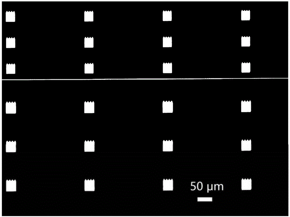
Examples
Embodiment
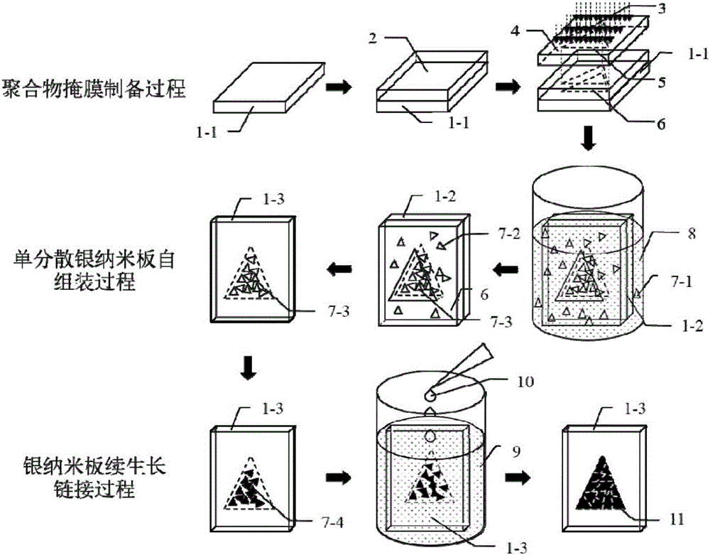
[0036] Step 1: Polymer mask preparation process
[0037] Spin-coat the UV-sensitive polymer on the silicon wafer, and transfer the two-dimensional pattern array on the mask plate to the UV-sensitive polymer after ultraviolet exposure and development, so as to obtain a polymer mask corresponding to the two-dimensional pattern array;
[0038] Step 2: Self-assembly process of monodisperse silver nanoplates
[0039] A high-yield silver nanoplate solution was obtained by using the seed crystal method; 10 mL of high-yield silver nanoplate solution was centrifuged twice at 8000 rpm; deionized water was added to a solution volume of 10 mL, and the concentration of the silver element was prepared to be 1 mmol / L The initial solution; Add 1mL of polyvinylpyrrolidone solution with a concentration of 50mmol / L and 500μL of ascorbic acid solution with a concentration of 100mmol / L to the initial solution in turn, stir fully to obtain a self-assembly solution; The silicon wafer was immersed i...
PUM
 Abstract
Description
Claims
Application Information