Electron collector material and preparation method of electron collector

An electron collection and collector technology, which is applied to the collector of the transit time type electron tube, the manufacture of the electrode system, the manufacture of the discharge tube/lamp, etc., which can solve the difficulty of maintaining the vacuum of the HPM system and the small secondary electron emission coefficient. , vacuum system carbon pollution and other problems, to achieve the effect of high melting point, low atomic number, and improved bonding strength

Active Publication Date: 2018-06-15
NAT UNIV OF DEFENSE TECH
View PDF4 Cites 0 Cited by
  • Summary
  • Abstract
  • Description
  • Claims
  • Application Information

AI Technical Summary

Problems solved by technology

Graphite has the characteristics of electrical conductivity, thermal conductivity, high melting point, and low atomic number, and its secondary electron emission coefficient is small, which helps to improve the efficiency of the collector. However, the graphite material is porous, so it is more difficult to maintain the vacuum of the HPM system. In addition, graphite collection Extremely will generate carbon pollution in the vacuum system, which will lead to a decrease in the insulation of the device

Method used


Image

  • Electron collector material and preparation method of electron collector
  • Electron collector material and preparation method of electron collector
  • Electron collector material and preparation method of electron collector

Examples


Embodiment 1

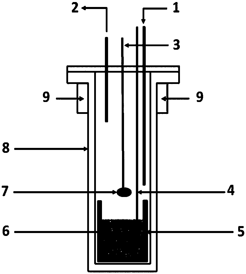
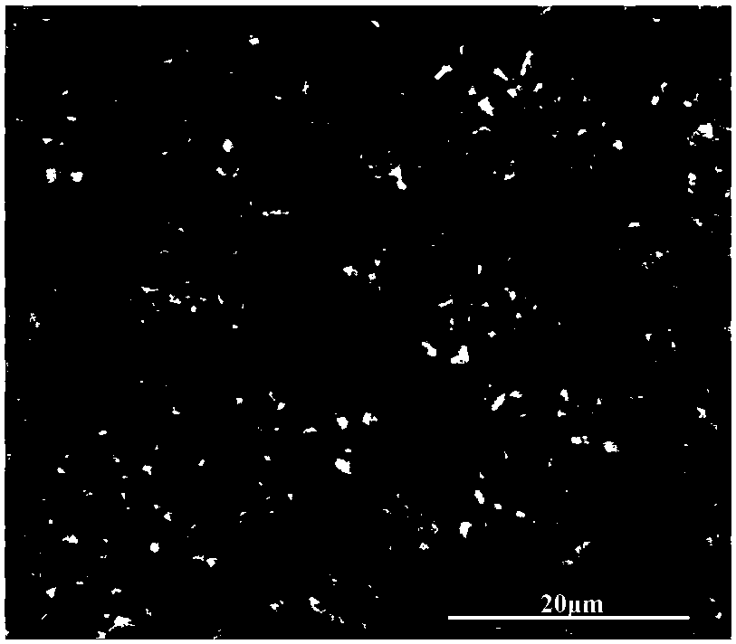
[0040] An electron collector material of the present invention includes a graphite matrix, and also includes TiC that penetrates into the interior of the graphite matrix relative to the surface of the graphite matrix, the TiC is formed by the in-situ reaction of elemental Ti and carbon in the graphite matrix, and the TiC is filled on the surface of the graphite matrix and in the internal pores.

[0041] In this embodiment, the TiC has a composition gradient from the surface of the graphite matrix to the interior of the graphite matrix, with a depth of about 120 μm.

[0042] A preparation method of electron collector of the present invention, comprises the following steps:

[0043] (1) Preparation of graphite collector body:

[0044] Using graphite as a raw material, according to the size requirements of the collector, the graphite block is processed into a flat graphite collector body 7 by conventional machining methods;

[0045] (2) Prepare collector preform:

[0046] (2.1...

Embodiment 2

[0054] An electron collector material of the present invention comprises a graphite matrix, TiC that penetrates into the interior of the graphite matrix relative to the surface of the graphite matrix and a TiC coating that covers the surface of the graphite matrix, and the TiC that penetrates into the interior of the graphite matrix is ​​elemental Ti and carbon in the graphite matrix Formed by in-situ reaction, the TiC coating is formed by the in-situ reaction of elemental Ti and carbon on the surface of the graphite substrate. The thickness of the TiC coating covering the surface of the graphite substrate is 10 μm to 15 μm, and there is a gradient of TiC infiltrating from the surface of the graphite substrate into the interior of the graphite substrate, with a depth of about 400 μ to 430 μm, and is filled in the pores inside the graphite substrate.

[0055] A preparation method of electron collector of the present invention, comprises the following steps:

[0056] (1) Prepara...

Embodiment 3

[0066] An electron collector material of the present invention comprises a graphite matrix, TiC that penetrates into the interior of the graphite matrix relative to the surface of the graphite matrix and a TiC coating that covers the surface of the graphite matrix, and the TiC that penetrates into the interior of the graphite matrix is ​​elemental Ti and carbon in the graphite matrix Formed by in-situ reaction, the TiC coating is formed by the in-situ reaction of elemental Ti and carbon on the surface of the graphite substrate. The thickness of the TiC coating covering the surface of the graphite substrate is 28 μm to 30 μm, and the content of TiC infiltrated from the surface of the graphite substrate to the interior of the graphite substrate has a gradient of decreasing content, with a depth of 415 μm to 430 μm, and is filled in the pores on the surface and inside of the graphite substrate.

[0067] A preparation method of electron collector of the present invention, comprises...


PUM

PropertyMeasurementUnit
depthaaaaaaaaaa
thicknessaaaaaaaaaa
depthaaaaaaaaaa

Abstract

The invention discloses an electron collector material and a preparation method of an electron collector. The electron collector material comprises a graphite substrate and TiC, wherein the TiC infiltrates the inside of the graphite substrate relative to the surface of the graphite substrate; and the TiC is formed by in-situ reaction of elemental Ti and carbon in the graphite substrate and is formed on the surface of the graphite substrate, and holes in the graphite substrate are filled with the TiC. The preparation method of the electron collector comprises the following steps of (1) preparation of a collector preform, namely mixing a titanium source with a molten salt medium, heating a mixture to a molten state in an inert atmosphere to obtain the molten mixture, immersing a graphite collector blank into the molten mixture and taking out the graphite collector blank for cooling to obtain the collector preform; and (2) sintering, namely sintering the collector preform obtained in the step (1) to obtain the electron collector. The electron collector material has the advantages of electron bombardment resistance, good cleanliness, long service life, good thermal conductivity, good conductivity and the like, and the preparation method of the electron collector is simple in process, low in cost and high in operability.

Description

technical field [0001] The invention belongs to the technical field of vacuum electronics, and in particular relates to an electron collector material and a preparation method of the electron collector. Background technique [0002] High Power Microwave (HPM: High Power Microwave) is generated by exchanging beam energy in a certain electromagnetic structure through a high-current electron beam. Due to the low energy conversion efficiency of the electron beam, the electron beam carrying most of the remaining energy needs to collected by the collector. The high-current electrons gradually lose energy through the interaction with the collector material, and finally deposit inside the material, thereby realizing the collection of the electron beam. The collector is repeatedly bombarded by high-current electron beams for a long time, which will cause electron emission, bremsstrahlung and serious temperature rise or even melting on the surface of the collector. The temperature r...

Claims


Application Information

Patent Timeline
Patent Type & Authority Patents(China)
IPC IPC(8): H01J23/027H01J9/02
CPCH01J9/02H01J23/027
Inventor 万红华叶陈彬白书欣
Owner NAT UNIV OF DEFENSE TECH
Why Eureka
Try Eureka