Quantum conductance effect based memristor and preparation and modulation method and application thereof

A modulation method and memristor technology, applied in electrical components and other directions, can solve problems such as difficult control, reduced chip integration, and easy resistance drift, and achieve the effects of increasing device density, overcoming resistance drift, and increasing storage capacity.

Inactive Publication Date: 2017-05-10
HUAZHONG UNIV OF SCI & TECH
View PDF3 Cites 9 Cited by
  • Summary
  • Abstract
  • Description
  • Claims
  • Application Information

AI Technical Summary

Problems solved by technology

[0003] The disadvantage of the above-mentioned solution for realizing multi-value storage is that additional constraints increase the difficulty of compatibility with traditional CMOS technology, and complex peripheral circuits increase the power consumption of the entire system and reduce the integration of the chip. More importantly, , the multi-value implemented by these schemes, its resistance value is easy to drift and difficult to control, which leads to unstable storage

Method used


Image

  • Quantum conductance effect based memristor and preparation and modulation method and application thereof
  • Quantum conductance effect based memristor and preparation and modulation method and application thereof
  • Quantum conductance effect based memristor and preparation and modulation method and application thereof

Examples


Embodiment 1

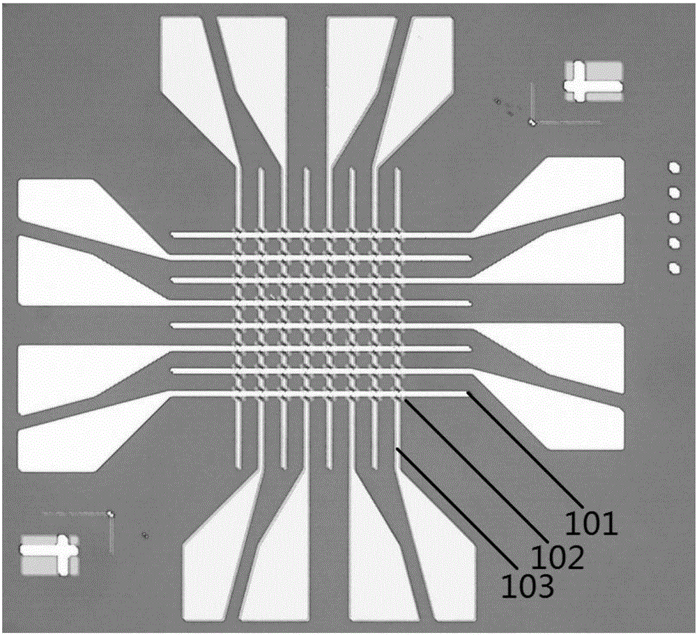
[0073] The memristor based on the quantum conductance effect provided in Example 1 is a Pt / HfO with an 8*8crossbar array structure x / Ti quantum conductance memristor, whose structure is as figure 1 shown; where the bottom electrode is Pt with a thickness of 150nm, and the functional layer is HfO with a thickness of 25nm x , 1.6

[0074] The following specifically describes the preparation method of the memristor based on the quantum conductance effect of embodiment 1; the specific steps are as follows:

[0075] (1) The first step:

[0076] (1.1) Photolithography: In the long thin SiO 2 One or more strip-shaped lower electrode patterns are prepared by a photolithography process on the Si substrate of the insulating layer;

[0077] Among them, the photolithography process includes: the steps of uniform glue, pre-baking, pre-exposure, post-baking, post-exposure, developing, coating, and stripping;

[0078] Sputtering...

Embodiment 2

[0097] The memristor based on the quantum conductance effect provided in Example 2 has a three-layer structure of a lower electrode, a functional layer and an upper electrode; wherein the material of the lower electrode is Pt with a thickness of 150nm; the functional layer is HfO with a thickness of 15nm x , 2

[0098] The following specifically describes the preparation method of the memristor based on the quantum conductance effect of embodiment 2; the specific steps are as follows:

[0099] (1) the first step;

[0100] Photolithography: The photolithography process has a total of eight steps: coating, pre-baking, pre-exposure, post-baking, post-exposure, development, coating, stripping, and photolithography to produce strip-shaped lower electrode patterns;

[0101] Sputtering: On the Si substrate with a thin SiO2 insulating layer, the Pt lower electrode is prepared by magnetron sputtering, with a thickn...


PUM


Abstract

The invention discloses a quantum conductance effect based memristor and a preparation and modulation method and application thereof. The memristor includes an upper electrode, a function layer and a lower electrode and has an MIM crossbar structure. Through regulating the proportion of argon and oxygen, function layer material having different thicknesses and oxygen vacancy is prepared. During modulation, conductive fiber states of the function layer are regulated accurately by adopting a voltage scanning or pulse scanning method and the size of the conductive fibers is controlled within an atomic scale, so that discontinuous conducting behaviors in a number which is the integral multiple of a unit conducting value are obtained and conducting quantization of the memristor is realized. Through exacting different quantum states of the memristor, resistance corresponding to the different quantum states is taken as different impedance for device storage, so that multi-value storage is realized. Besides, a function of the memristor of simulating nerve cell synapsis is implemented. The memristor eliminates influence of impedance drifting caused by dispersion change of conductance states on device application and realizes the quantum storage device with smaller working current, higher storage density, faster reading speed and no loss after power failure.

Description

technical field [0001] The invention belongs to the technical field of microelectronic devices, and more specifically relates to a memristor based on quantum conductance effect and its preparation and modulation method and application. Background technique [0002] At this stage, the methods for realizing multi-value storage through memristors mainly include: changing the limit current in the SET process or changing the cut-off voltage in the RESET process during modulation; for the method of changing the limit current in the SET process, the In / V voltage scanning or pulse scanning mode, by limiting the maximum current passed by the device when the SET voltage is applied, the resistance value of the device is controlled to realize multi-value storage; for changing the cut-off voltage in the RESET process, it is in I / In the V voltage scanning or pulse scanning mode, by adjusting the amplitude of the negative pulse, the degree of breakage of the conductive filament is limite...

Claims


Application Information

Patent Timeline
Patent Type & Authority Applications(China)
IPC IPC(8): H01L45/00
CPCH10N70/00
Inventor 孙华军何维凡钟姝婧缪向水
Owner HUAZHONG UNIV OF SCI & TECH
Why Eureka
Try Eureka