Bulk-heterojunction perovskite thin film, production method thereof and solar cell

A solar cell and bulk heterojunction technology, applied in the field of solar cells, can solve the problems that are not conducive to large-scale production and yield control, increase the difficulty of perovskite film preparation, and film charge recombination, so as to avoid high temperature sintering process, Strong electron extraction ability, reducing the effect of charge recombination

Active Publication Date: 2017-05-10
SHANGHAI INST OF CERAMIC CHEM & TECH CHINESE ACAD OF SCI
View PDF6 Cites 36 Cited by
  • Summary
  • Abstract
  • Description
  • Claims
  • Application Information

AI Technical Summary

Problems solved by technology

If there are many pinhole defects in the prepared film, it is easy to cause the recombination of charges in the film, which seriously affects the performance

Method used


Image

  • Bulk-heterojunction perovskite thin film, production method thereof and solar cell
  • Bulk-heterojunction perovskite thin film, production method thereof and solar cell

Examples


preparation example Construction

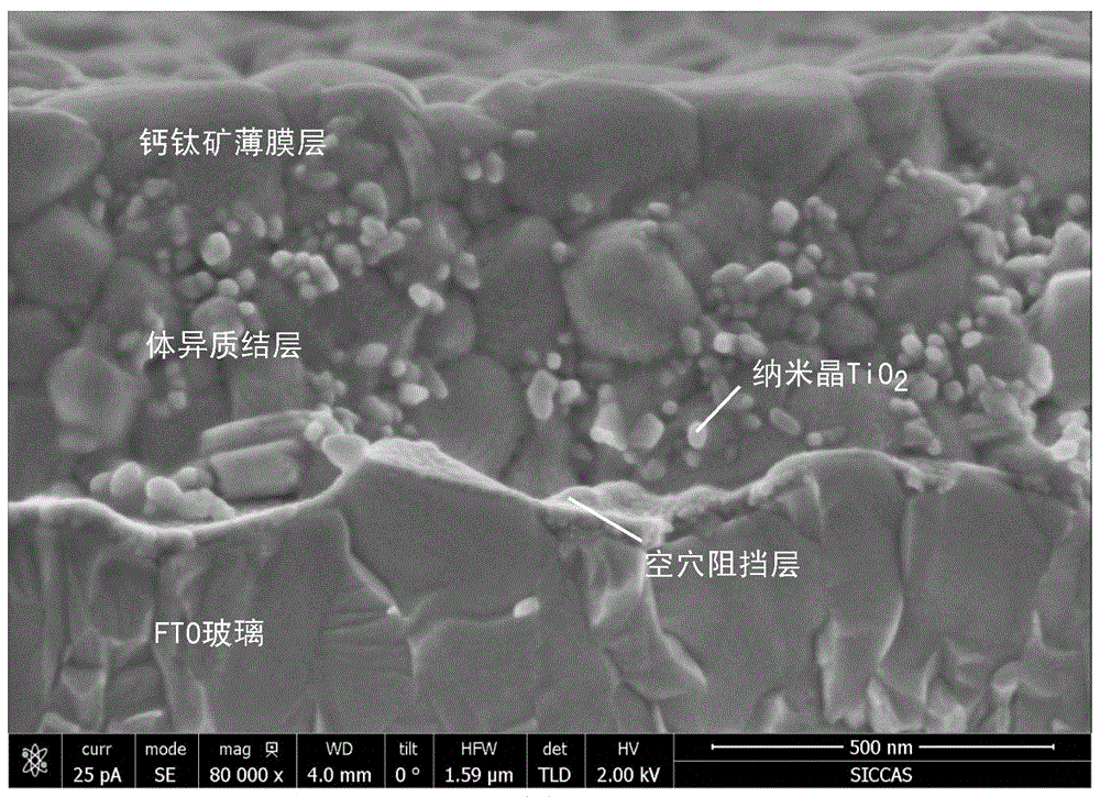
[0027] The invention relates to a bulk heterojunction perovskite film, a corresponding perovskite solar cell and a preparation method thereof. By coating the prepared perovskite precursor solution and perovskite / electron acceptor material dispersion on the substrate, a bulk heterojunction precursor film is formed, and by crystallizing the bulk heterojunction precursor film, The bulk heterojunction perovskite thin film of the present invention is obtained. The bulk heterojunction film of the present invention adopts perovskite material as the electron donor material, and the electron acceptor material is located at the grain boundary of the perovskite polycrystalline film, and a dense perovskite film layer is formed on the surface of the bulk heterojunction , compared with the traditional perovskite film, the preparation method is simpler, and the film quality is easier to control, which overcomes the problems of complex traditional structure and process and higher requirements...
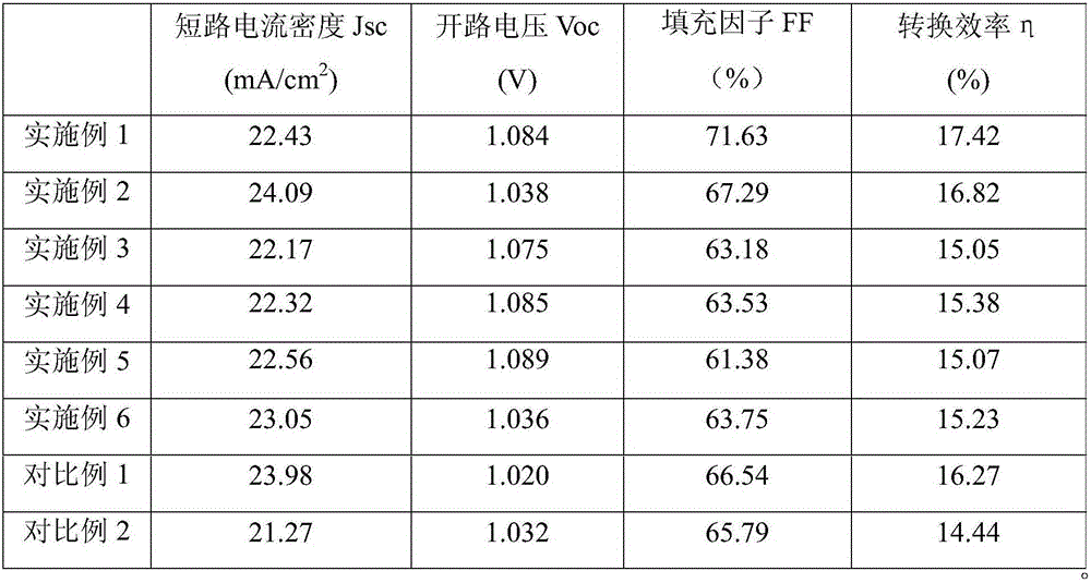
Embodiment 1

[0066] Synthesis of TiO by Hydrothermal Method 2 Nanocrystalline: Add 150mL tetrabutyl titanate into a glass reactor filled with 0.1moL / L dilute nitric acid solution (1000mL) under vigorous stirring, hydrolyze to form a white precipitate, then heat the reactor to 120°C and keep stirring Incubate for 8 hours to degumming and concentrate. The resulting sol was transferred into a titanium autoclave and subjected to hydrothermal treatment at 260 °C for 12 hours to obtain TiO 2 Nanocrystalline. Obtained TiO 2 The particle size of the nanocrystals is about 20nm;

[0067] (1) Preparation of perovskite / electron acceptor material dispersion. First prepare TiO 2 DMF dispersion: the hydrothermally synthesized TiO 2 The nanocrystals were washed with deionized water, ethanol and DMF to remove impurities, and then dispersed in DMF to form a dispersion liquid for later use. Then, the PbI 2 , MAI and DMSO were dissolved in DMF at a ratio of 1:1:1 and stirred thoroughly to obtain a per...

Embodiment 2

[0074] (1) Preparation of perovskite / electron acceptor material dispersion. First prepare TiO 2 DMF dispersion: the hydrothermally synthesized TiO 2 The nanocrystals were washed with deionized water, ethanol and DMF to remove impurities, and then dispersed in DMF to form a dispersion liquid for later use. Then, the PbI 2 , MAI and DMSO were dissolved in DMF at a ratio of 1:1:1 and stirred thoroughly to obtain a perovskite precursor solution (MAPbI 3 ), and then mix the perovskite precursor solution with TiO 2 DMF dispersion in a certain proportion (MAPbI 3 with TiO 2 Molar ratio is 10:1) mixed to obtain MAPbI 3 / TiO 2 Nanocrystalline precursor dispersion;

[0075] (2) Cleaning of the conductive substrate. With embodiment 1;

[0076] (3) Preparation of hole blocking layer. With embodiment 1;

[0077] (4) Preparation of perovskite heterojunction active layer. Dropwise addition of MAPbI on the substrate of FTO / hole blocking layer 3 / TiO 2 Nanocrystalline precursor ...


PUM

PropertyMeasurementUnit
Thicknessaaaaaaaaaa
Thicknessaaaaaaaaaa
Thicknessaaaaaaaaaa

Abstract

The invention relates to a bulk-heterojunction perovskite thin film, a production method thereof and a solar cell. The bulk-heterojunction perovskite thin film comprises a bulk-heterojunction layer and a perovskite thin film layer located on the surface of the bulk-heterojunction layer, wherein the bulk-heterojunction layer comprises a perovskite polycrystalline thin film serving as an electron donor material and an electron acceptor material located at the crystal boundary position of the perovskite polycrystalline thin film. The bulk-heterojunction perovskite thin film has the advantages that when the bulk-heterojunction perovskite thin film is applied to the perovskite solar cell, the bulk-heterojunction perovskite thin film can replace an existing mesoporous electron transfer layer and an existing perovskite light absorption layer, and accordingly the structure of the cell can be simplified; the high-temperature sintering process needed by the production of the independent mesoporous layer can be omitted, and the bulk-heterojunction perovskite thin film is suitable for producing the efficient and flexible perovskite solar cell on a plastic substrate.

Description

technical field [0001] The invention belongs to the technical field of solar cells, in particular to a method for preparing a thin film for a solar cell, and more specifically, to a bulk heterojunction perovskite thin film, a corresponding perovskite solar cell and a preparation method thereof. Background technique [0002] With the development of human society, the demand for energy is increasing day by day. As a clean and non-polluting energy source, solar energy has received extensive attention and in-depth research at home and abroad. Solar cells based on organic-inorganic hybrid perovskite films are a new type of solar cells developed in recent years, and their advantages are very prominent: 1. The preparation process of organic-inorganic hybrid perovskite materials is simple and the cost is low; 2. It has an adjustable band gap; 3. Balanced electron-hole mobility, high quantum luminous efficiency and large defect tolerance; 4. It can be made into a semi-transparent ba...

Claims


Application Information

Patent Timeline
IPC IPC(8): H01L51/42H01L51/48
CPCH10K30/30H10K30/35H10K30/353Y02E10/549
Inventor 杨松旺邵君刘岩
Owner SHANGHAI INST OF CERAMIC CHEM & TECH CHINESE ACAD OF SCI
Why Eureka
Try Eureka