Broadband efficient GaN-based LED chip based on surface plasma effect and preparation method thereof

A surface plasmon and LED chip technology, applied in semiconductor devices, electrical components, nanotechnology, etc., can solve problems such as reducing composite life, and achieve the effects of improving current density, reducing loss, and improving modulation bandwidth

Active Publication Date: 2017-05-31
SOUTH CHINA UNIV OF TECH
View PDF6 Cites 9 Cited by
  • Summary
  • Abstract
  • Description
  • Claims
  • Application Information

AI Technical Summary

Problems solved by technology

When the frequency of the excitons matches the resonant frequency of the SP, the rate at which the exciton energy couples to the SP mode is much greater than the other two decay processes, thereby reducing the recombination lifetime of minority carriers and increasing the modulation bandwidth

Method used


Image

  • Broadband efficient GaN-based LED chip based on surface plasma effect and preparation method thereof
  • Broadband efficient GaN-based LED chip based on surface plasma effect and preparation method thereof
  • Broadband efficient GaN-based LED chip based on surface plasma effect and preparation method thereof

Examples


Embodiment 1

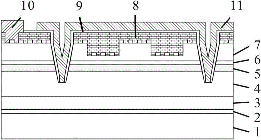
[0087] A broadband high-efficiency GaN-based LED chip based on the surface plasmon effect, with a structure such as Figure 1-8 shown.

[0088] A micro-nano composite structure is prepared on the surface of the p-GaN of the flip-chip LED chip; the microstructure is a circular frustum with a triangular lattice distribution, the lattice constant is 2 μm, the diameter of the upper bottom of the circular frustum is 1.3 μm, and the diameter of the lower bottom is 1 μm. The nanostructure is a cylinder of hexagonal lattice distribution distributed on the entire p-GaN surface, the lattice constant is 100 nm, the height and diameter of the cylinder are 50nm, and the bottom of the cylinder located in the recess of the microstructure is 10 away from the top of the quantum well 5 nm; a metal mirror layer 8 is prepared on the p-GaN layer 7 to form a micro-nano composite metal structure.

[0089] Preparation of the above-mentioned broadband high-efficiency GaN-based LED chip based on the ...

Embodiment 2

[0101] A broadband high-efficiency GaN-based LED chip based on the surface plasmon effect, with a structure such as Figure 2-7 shown.

[0102] A micro-nano composite structure is prepared on the surface of the p-GaN of the flip-chip LED chip; the micron structure is a one-dimensional grating with a lattice constant of 3 μm, the diameter of the upper bottom of the grating hole is 1.8 μm, and the diameter of the lower bottom is 1.5 μm. The bottom is 30 nm away from the top of the quantum well 5; the nanostructure is located at the bottom of the microstructure recess, and is an irregular structure randomly distributed, the height and width of the irregular structure are 50nm, and the gap between the irregular structures is 200nm; A metal mirror layer 8 is prepared on the GaN layer 7 to form a micro-nano composite metal structure.

[0103] To prepare the above-mentioned broadband high-efficiency GaN-based LED chip based on the surface plasmon effect, the preparation process is a...

Embodiment 3

[0113] A broadband high-efficiency GaN-based LED chip based on the surface plasmon effect, with a structure such as Figure 3-8 shown.

[0114] A micro-nano composite structure is prepared on the surface of the p-GaN of the flip-chip LED chip. The microstructure is a cuboid with a hexagonal lattice distribution, the lattice constant is 4 μm, and the side length of the cuboid is 2 μm. The nanostructure is a circular truncated triangular lattice distribution distributed on the entire p-GaN surface, the lattice constant is 250 nm, the height and diameter of the circular truncated are 125 nm, and the bottom of the circular truss located in the recess of the microstructure is 40° away from the top of the quantum well 5 nm. A metal mirror layer 8 is prepared on the p-GaN layer 7 to form a micro-nano composite metal structure.

[0115] Preparation of the above-mentioned broadband high-efficiency GaN-based LED chip based on the surface plasmon effect, the preparation process diagra...


PUM


Abstract

The invention discloses a broadband efficient GaN-based LED chip based on surface plasma effect and a preparation method thereof. The broadband efficient GaN-based LED chip is an inversion structure, and successively comprises a substrate, a buffer layer, an unintentional doping GaN layer, a n-GaN layer, a quantum well layer, an electronic barrier layer, a p-GaN layer, a metal reflector layer, a passivation layer, a p-electrode layer, a n-electrode layer, a p-electrode hole and a n-electrode hole from bottom to top. The bottom face, connected with the surface of the p-GaN layer, of the metal reflector layer is provided with a micron-nano compound metal structure. The micron metal structure comprises alternately installed bulge part and groove part. The bulge part is extended to the adjacent place of the quantum well, and the efficient SP-MQW coupling is realized. The p-GaN surface is covered by the groove part, so the p-GaN layer has enough thickness for injecting the hole. The nano-metal structure is distributed on the division surface of the micron-metal structure and the p-GaN.

Description

technical field [0001] The invention relates to the field of GaN-based LED chips for visible light communication, in particular to a wide-band and high-efficiency GaN-based LED chip based on the surface plasmon effect and a preparation method thereof. Background technique [0002] Visible light communication uses high-speed blinking LEDs as a signal source. When the flickering frequency of the LED exceeds the response limit of the human eye, the signal source can be used as a light source in lighting, display, backlight and other fields at the same time. With the wide application of LEDs in the above fields, LED chips with high luminous efficiency and high modulation bandwidth, which have both the functions of light source and signal source, have become a research hotspot. [0003] The modulation bandwidth of the LED chip is mainly affected by the recombination lifetime of minority carriers in the active region and the RC bandwidth, where R and C are the equivalent resistan...

Claims


Application Information

Patent Timeline
Patent Type & Authority Applications(China)
IPC IPC(8): H01L33/20H01L33/06H01L33/00B82Y40/00
CPCH01L33/0075H01L33/06H01L33/20B82Y40/00H01L33/382H01L33/387H01L33/405H01L33/32H01L33/44H01L33/22H01L2933/0016H01L2933/0025H01L33/46
Inventor 黄华茂王洪胡晓龙杨倬波文如莲施伟
Owner SOUTH CHINA UNIV OF TECH
Why Eureka
Try Eureka