Eureka AIR delivers breakthrough ideas for toughest innovation challenges, trusted by R&D personnel around the world.

An ultra-broadband absorption heterojunction solar cell

A solar cell and heterojunction technology, applied in circuits, electrical components, photovoltaic power generation, etc., can solve the problems of low light absorption efficiency in the visible light band and unusable light energy, and achieve the effect of improving photoelectric conversion efficiency

Active Publication Date: 2018-12-14
SOUTHEAST UNIV
View PDF5 Cites 0 Cited by
  • Summary
  • Abstract
  • Description
  • Claims
  • Application Information

AI Technical Summary

Problems solved by technology

[0005] Technical problem: The purpose of this invention is to solve the technical problems of low light absorption efficiency in the visible light band of existing heterojunction solar cells, and the inability to utilize light energy lower than the semiconductor band gap, and propose a heterojunction solar cell with ultra-broadband absorption , enhance the spectral response of the battery in the ultraviolet to infrared ultra-broadband, thereby improving the photoelectric conversion efficiency of the battery

Method used


Image

  • An ultra-broadband absorption heterojunction solar cell
  • An ultra-broadband absorption heterojunction solar cell
  • An ultra-broadband absorption heterojunction solar cell

Examples


example example 1

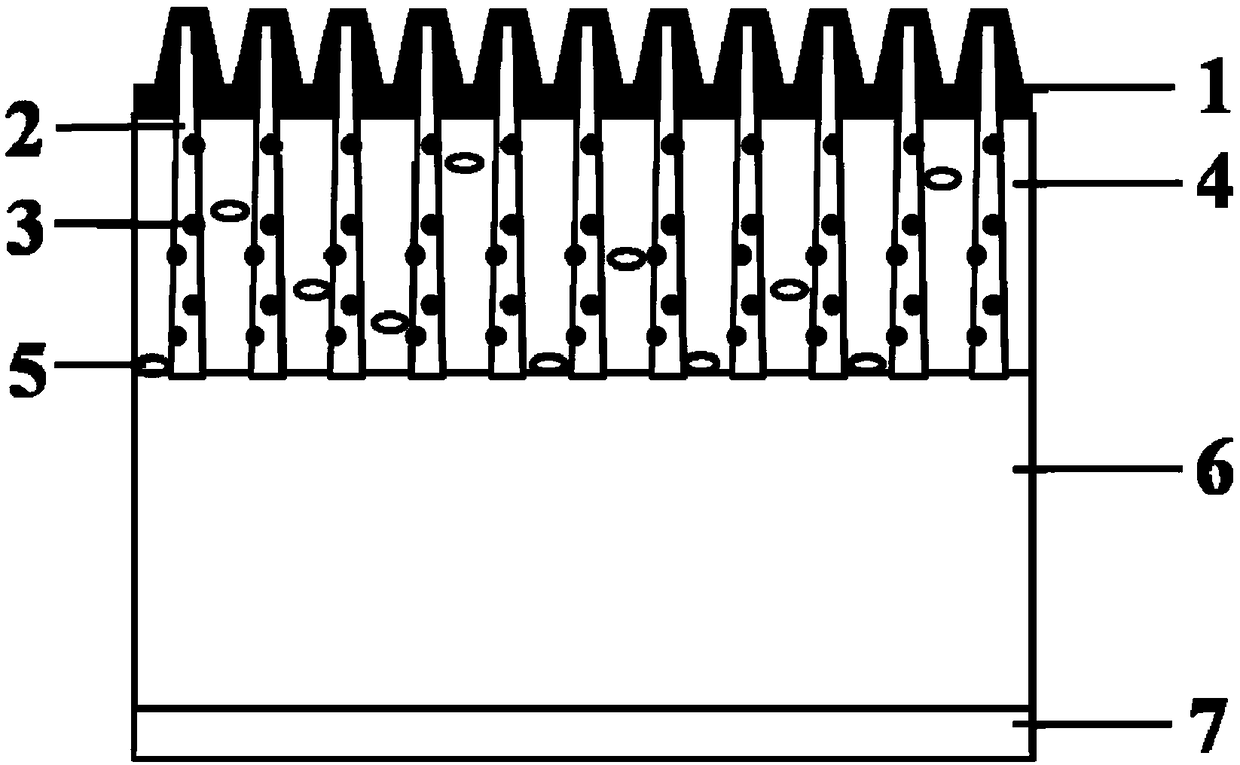
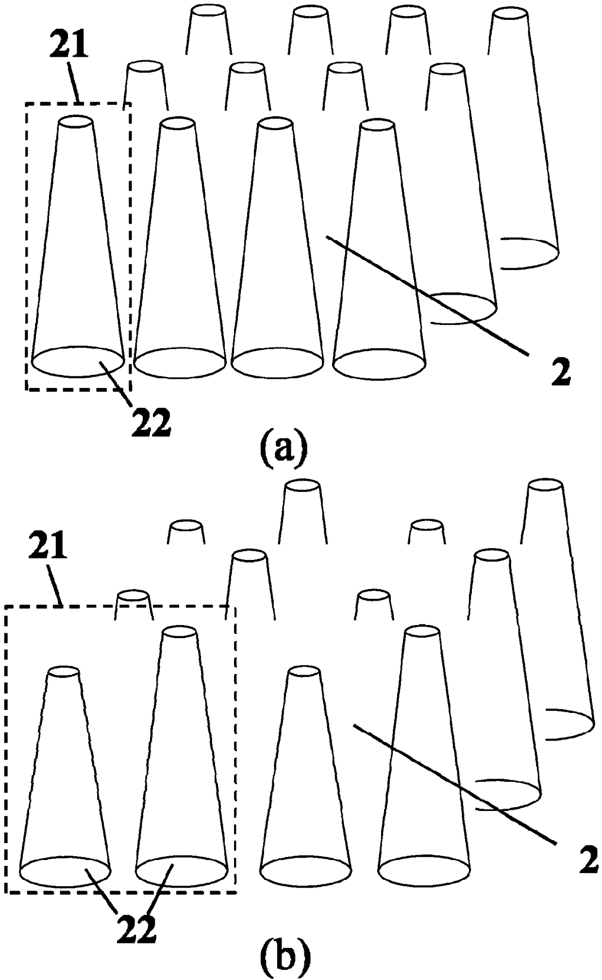
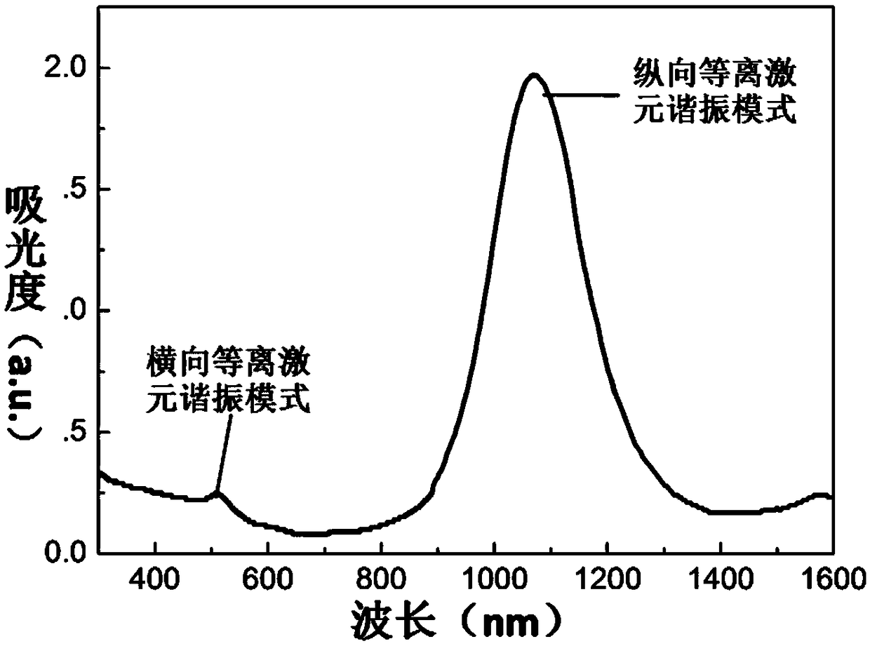
[0038] In the battery structure, the nanocone unit structure has only one nanocone with structural parameters (such as figure 2 a), the spacing is 50 nanometers, the material of the nanocone is gold, the width of the tip is 15 nanometers, the width of the bottom is 15 nanometers, and the height is 100 nanometers. The transverse plasmon resonance absorption and longitudinal plasmon absorption spectra are as follows image 3 As shown, its transverse plasmon resonance absorption peak is located at about 520 nanometers, and its longitudinal plasmon resonance absorption peak is located at about 1100 nanometers; the material of the transparent conductive front electrode is indium tin oxide ITO with a thickness of 100 nanometers; the down-conversion quantum The dot material is cadmium selenide quantum dot material; the organic conductive polymer layer material is poly 3,4-ethylenedioxythiophene-polystyrene sulfonic acid PEDOT:PSS, with a thickness of 70 nanometers; the plasmonic ligh...

example example 2

[0040] In the battery structure, the nanocone unit structure has two kinds of nanocones with structural parameters, and the arrangement of the three nanocones is as follows: figure 2 As shown in b, the material of the nanocone is silver, the width of the tip is 10 nanometers, the width of the bottom is 15 nanometers, and the height is 120 nanometers and 140 nanometers respectively. The distance between different nanocones in the unit structure is 50 nanometers, and the distance between the nanocone array units is 130 nanometers ; down-converting nanostructures to samarium Sm 3+ Doped with quantum dot materials; the material of the transparent conductive front electrode is aluminum-doped zinc oxide AZO, with a thickness of 120 nanometers; the material of the organic conductive polymer layer is poly-3-octylthiophene P3OT, with a thickness of 80 nanometers; plasmonic light trapping The palladium decahedron is selected as the structure, and the size is 40 nanometers; the semicond...


PUM


Abstract

The invention discloses a heterojunction solar cell with ultra-broadband absorption. The specific structure includes a transparent conductive front electrode, a two-dimensional nanocone array superstructure, a down-conversion nanostructure, a plasmon light-trapping structure, and an organic conductive polymer layer. , a semiconductor material layer and a back electrode. The cell uses down-conversion nanostructures to achieve photon cutting of ultraviolet light, converting ultraviolet light into visible light; using a two-dimensional nanocone array superstructure with tip plasmon excitation effect, and plasmon light trapping structure, in visible light The wavelength band enhances the light absorption of the heterojunction formed by the organic conductive polymer and the semiconductor; and uses the heterojunction formed by the two-dimensional nanocone array superstructure and the semiconductor to make the device absorb and convert infrared light smaller than the semiconductor band gap, and enhance the battery infrared The spectral response within the band. The battery has high photoelectric conversion efficiency in the ultraviolet to infrared ultra-wide spectrum range, and has the advantages of low cost, simple process, high specific efficiency and the like.

Description

technical field [0001] The invention is specifically an ultra-broadband absorption heterojunction solar cell. Belonging to the technical field of solar cell manufacturing, Background technique [0002] With the depletion of fossil energy, solar cell technology has developed rapidly, and is expected to replace traditional fossil energy and become the mainstream energy in the future. In the research of solar cells, higher efficiency and lower cost cells are an eternal theme. Traditional solar cells, mainly made of semiconductor raw materials, need to be doped to form a PN junction, but solar cells based on PN junctions are difficult to realize the energy utilization and conversion of photons with energy lower than the semiconductor band gap, which not only limits the improvement of the photoelectric conversion efficiency of the cell , but also cause aging or even rupture of solar cells due to the thermal effect of infrared light. In addition, in the processing of traditiona...

Claims


Application Information

Patent Timeline
Patent Type & Authority Patents(China)
IPC IPC(8): H01L51/42H01L51/44
CPCH10K30/10H10K30/87Y02E10/549
Inventor 张彤苏丹张晓阳吴静远王善江
Owner SOUTHEAST UNIV
Why Eureka
Eureka Blog
Learn More