A method of manufacturing a semiconductor device

A manufacturing method and semiconductor technology, applied in semiconductor/solid-state device manufacturing, electrical components, circuits, etc., can solve problems affecting product yield and performance, wafer scrapping, etc., to improve yield and performance, and increase deposition temperature. Effect

Active Publication Date: 2019-12-03
CSMC TECH FAB2 CO LTD
View PDF1 Cites 0 Cited by
  • Summary
  • Abstract
  • Description
  • Claims
  • Application Information

AI Technical Summary

Problems solved by technology

Among them, the tungsten silicide deposition process is a crucial process in the semiconductor process of 0.35 μm or more, which directly affects the polysilicon resistance. In the existing process, a doped polysilicon layer is often deposited on the tungsten silicide , online products found that after the high-temperature annealing process after the tungsten silicide deposition process (for example, high temperature 1035 degrees rapid thermal annealing RTA after ion implantation), the edge stress of the wafer (wafer) changes, making the tungsten silicide change from the normal stress before annealing to Negative stress after annealing, while the doped polysilicon layer on it changes from the negative stress of the principle to the positive stress after annealing, such as figure 1 As shown, peeling occurs between tungsten silicide and its upper layer of polysilicon, which affects product yield and performance, and eventually makes the wafer scrap

Method used


Image

  • A method of manufacturing a semiconductor device
  • A method of manufacturing a semiconductor device
  • A method of manufacturing a semiconductor device

Examples


Embodiment 1

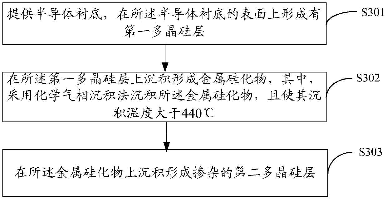
[0035] As an example, the manufacturing method of the semiconductor device of the present invention includes the following steps:

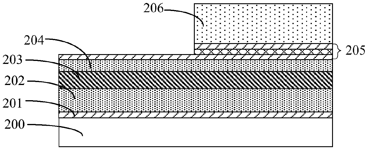
[0036] First, step S301 is performed to provide a semiconductor substrate 200 on which a first polysilicon layer 202 is formed.

[0037] Such as figure 2 As shown, wherein, the semiconductor substrate 200 can be at least one of the materials mentioned below: silicon, silicon-on-insulator (SOI), silicon-on-insulator (SSOI), silicon-germanium-on-insulator (S -SiGeOI), silicon germanium on insulator (SiGeOI) and germanium on insulator (GeOI), etc.

[0038] In addition, an active region may be defined on the semiconductor substrate 200 . Other active devices may also be included on the active area, which are not marked in the shown figures for convenience.

[0039] A gate dielectric layer 201 is formed on the semiconductor substrate 200, wherein the gate dielectric layer 201 can be selected from common dielectric materials in the field, for exampl...

Embodiment 2

[0062] Embodiment 2 of the present invention provides a method for manufacturing a semiconductor device, which specifically includes the following steps:

[0063] continue to refer figure 2 Firstly, a semiconductor substrate 200 is provided, and a first polysilicon layer 202 is formed on the surface of the semiconductor substrate 200 .

[0064] Exemplarily, a gate dielectric layer 201 is formed on the semiconductor substrate 200,

[0065] Wherein, the gate dielectric layer 201 can be selected from commonly used dielectric materials in the field, for example, oxide can be selected. The first polysilicon layer 202 is formed on the surface of the gate dielectric layer 201 .

[0066] Wherein, this step is basically the same as the step in the first embodiment above, and will not be repeated here.

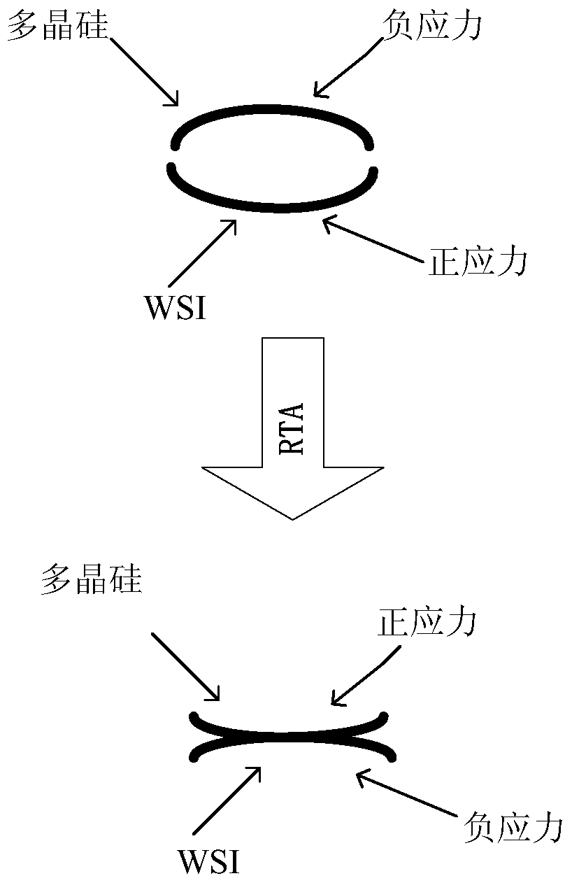
[0067] Next, a metal silicide 203 is deposited on the first polysilicon layer 202 , wherein the metal silicide 203 is deposited by chemical vapor deposition at a deposition temperat...


PUM

PropertyMeasurementUnit
thicknessaaaaaaaaaa
thicknessaaaaaaaaaa

Abstract

The invention provides a method for manufacturing a semiconductor device and relates to the technical field of a semiconductor. The method comprises steps that a semiconductor substrate is provided, and a first polysilicon layer is formed on the surface of the semiconductor substrate; metal silicide is formed on the first polysilicon layer through deposition, the metal silicide is deposited in an chemical vapor deposition method, and deposition temperature is made to be greater than 440 DEG C; a second doped polysilicon layer is formed on the metal silicide through deposition. According to the manufacturing method, through enhancing the deposition temperature of the metal silicide and prolonging the deposition time non-doped polysilicon in the polysilicon layer on the metal silicide, stress of corresponding material layers is reduced, a problem of peeling of the metal silicide and the upper-layer polysilicon layer caused by change of stress generated in a later annealing process can be avoided, and thereby the yield and performance of devices are improved.

Description

technical field [0001] The invention relates to the technical field of semiconductors, in particular to a method for manufacturing a semiconductor device. Background technique [0002] In some semiconductor devices using polysilicon gates, in order to improve device performance, it is generally desired that the gate resistance can be relatively small. There are generally several ways to reduce the polysilicon gate resistance: increasing the thickness of polysilicon; doping polysilicon; depositing metal silicide on polysilicon, etc. Among them, the tungsten silicide deposition process is a crucial process in the semiconductor process of 0.35 μm or more, which directly affects the polysilicon resistance. In the existing process, a doped polysilicon layer is often deposited on the tungsten silicide , online products found that after the high-temperature annealing process after the tungsten silicide deposition process (for example, high temperature 1035 degrees rapid thermal an...

Claims


Application Information

Patent Timeline
Patent Type & Authority Patents(China)
IPC IPC(8): H01L21/285
CPCH01L21/28506
Inventor 严琴
Owner CSMC TECH FAB2 CO LTD
Why Eureka
Try Eureka