Eureka AIR delivers breakthrough ideas for toughest innovation challenges, trusted by R&D personnel around the world.

Non-oxidized nano copper soldering paste for high-power chip packaging and preparation method of soldering paste

A chip packaging, high-power technology, used in welding equipment, manufacturing tools, welding media, etc., can solve the problem of poor electrical properties of nano-copper sintered body, mechanical properties of connection structures need to be improved, and nano-copper solder paste The scope of application is narrowed, etc. problems, to achieve the effect of simple and easy-to-obtain equipment, high service temperature and low cost

Active Publication Date: 2017-06-13
HARBIN INST OF TECH SHENZHEN GRADUATE SCHOOL +1
View PDF9 Cites 21 Cited by
  • Summary
  • Abstract
  • Description
  • Claims
  • Application Information

AI Technical Summary

Problems solved by technology

Although gold and silver have excellent electrical conductivity, due to the high cost of raw materials, it is difficult to popularize and apply them on a large scale, while copper not only has better electrical conductivity, but also has low cost, which is more suitable for huge electronic industry clusters
The problem is that the chemical properties of copper are lively and easy to oxidize. On the one hand, the existence of oxidation increases the sintering temperature of copper nanoparticles, which narrows the scope of application of nano-copper solder paste; on the other hand, it will make the electrical properties of nano-copper sintered Difference
Therefore, the existing nano-copper solder pastes all have the problems of high sintering temperature and poor conductivity, and the mechanical properties of the formed connection structure also need to be improved.

Method used


Image

  • Non-oxidized nano copper soldering paste for high-power chip packaging and preparation method of soldering paste

Examples


preparation example Construction

[0029] A preparation method for an oxidation-free nanometer copper solder paste used as high-power chip packaging, comprising the following steps:

[0030] (1) Configure a polyol solution mixed with a certain concentration of copper source and dispersant, and heat it to a certain temperature.

[0031] (2) Configure a polyol solution with a certain concentration of reducing agent and heat it to a certain temperature.

[0032] (3) The initial copper nanoparticles were synthesized by chemical reduction method.

[0033] (4) Prepare an anhydrous ethanol solution of a certain concentration of organic acid.

[0034] (5) Soak the synthesized primary copper nanoparticles in an organic acid solution of ethanol to remove the oxide layer on the surface of the primary copper nanoparticles.

[0035] (6) Mix the prepared surface oxide-free copper nanoparticles with an organic solvent, and obtain an oxidation-free nano-copper solder paste after stirring by mechanical stirring and a small pl...

Embodiment 1

[0052] Implementation example 1 A kind of oxidation-free nano-copper solder paste used as high-power chip packaging and its preparation method

[0053] Take 1 g of copper nanoparticles prepared by the chemical reduction method, mix with 2.5% formic acid in absolute ethanol solution, let stand for 10 min until the solution is separated, and centrifuge the copper nanoparticles. The precipitated copper nanoparticles are washed several times with absolute ethanol, and after the upper liquid becomes colorless and transparent, the nanoparticles are centrifugally precipitated to obtain oxide-free copper nanoparticles.

[0054] Mix the oxide-free copper nanoparticles and ethylene glycol at a mass ratio of 1:1, mechanically stir for 40 minutes, and then fully stir with a small planetary gravity mixer. After 50 seconds, an oxidation-free nano-copper solder paste is obtained.

[0055] Deposit the non-oxidative nano-copper paste on the DBC substrate by stencil printing, after drying, asse...

Embodiment 2

[0056] Implementation example 2 A kind of oxidation-free nano-copper solder paste used as high-power chip packaging and its preparation method

[0057] Take 1 g of copper nanoparticles prepared by the chemical reduction method, mix with 5% formic acid in absolute ethanol solution, let stand for 10 min until the solution is separated, and centrifuge the copper nanoparticles. The precipitated copper nanoparticles are washed several times with absolute ethanol, and after the upper liquid becomes colorless and transparent, the nanoparticles are centrifugally precipitated to obtain oxide-free copper nanoparticles.

[0058] Mix the oxide-free copper nanoparticles and ethylene glycol at a mass ratio of 1:1, mechanically stir for 40 minutes, and then fully stir with a small planetary gravity mixer. After 50 seconds, an oxidation-free nano-copper solder paste is obtained.

[0059] Deposit the non-oxidative nano-copper paste on the DBC substrate by stencil printing, after drying, assemb...


PUM

PropertyMeasurementUnit
Particle sizeaaaaaaaaaa
Resistivityaaaaaaaaaa
Shear strengthaaaaaaaaaa

Abstract

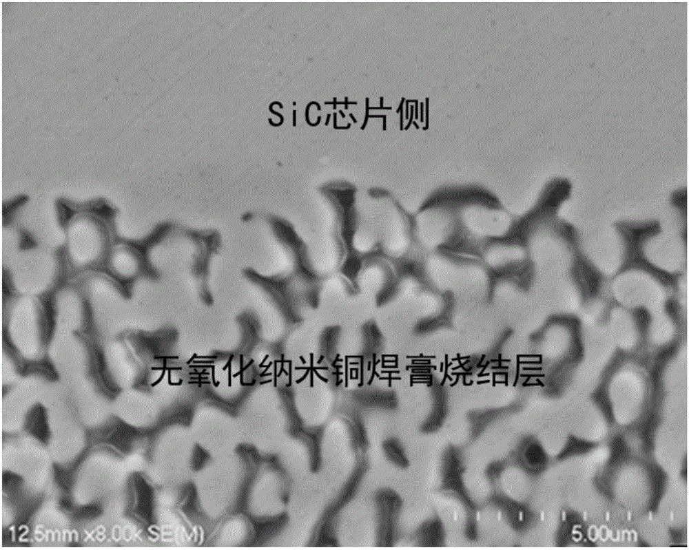
The invention provides non-oxidized nano copper soldering paste for high-power chip packaging and a preparation method of the soldering paste. Copper nanoparticles with the non-oxidized surfaces with the particle size being 30-60 mu m and an organic solvent are mixed in the mass ratio of 2:1-5:1, mechanical stirring and planet type gravity stirring are performed, and the nano copper soldering paste is obtained. The invention further provides the preparation method of the copper nanoparticles with the non-oxidized surfaces. The non-oxidized nano copper soldering paste prepared with the method has higher conductivity and better mechanical properties than common nano copper soldering paste and tin-lead solder. The preparation method is simple and practical and causes no environmental pollution and industrial popularization and application can be realized.

Description

technical field [0001] The invention belongs to the technical field of electronic packaging and interconnection materials, and relates to an oxidation-free nano-copper solder paste used for high-power chip packaging and a preparation method thereof. Background technique [0002] Microelectronic packaging provides interconnects, physical protection and mechanical support for semiconductor devices, enabling them to function under specific conditions. Therefore, packaging interconnect materials, which serve as a bridge between the chip and the rest of the system, play an important role in ensuring the continuity of device operation. In view of the operating temperature below 300°C, tin-based solder and conductive adhesive are often widely used in the packaging and interconnection of electronic components. However, in some special occasions such as automotive electronics, oil well drilling, and aerospace fields, the use temperature of devices is as high as 350°C. At this time, ...

Claims


Application Information

Patent Timeline
IPC IPC(8): B23K35/40
CPCB23K35/40
Inventor 李明雨刘敬东杨世华
Owner HARBIN INST OF TECH SHENZHEN GRADUATE SCHOOL
Why Eureka
Eureka Blog
Learn More