Electrode lead unit, vacuum photoelectric device and manufacturing method thereof
A technology of electrode leads and manufacturing methods, which is applied in the field of optoelectronic devices, can solve problems such as inability to meet the requirements of multi-electrode leads, and achieve the effects of avoiding device bursting or slow gas leakage, low cost, and small volume
- Summary
- Abstract
- Description
- Claims
- Application Information
AI Technical Summary
Problems solved by technology
Method used
Image
Examples
Embodiment Construction
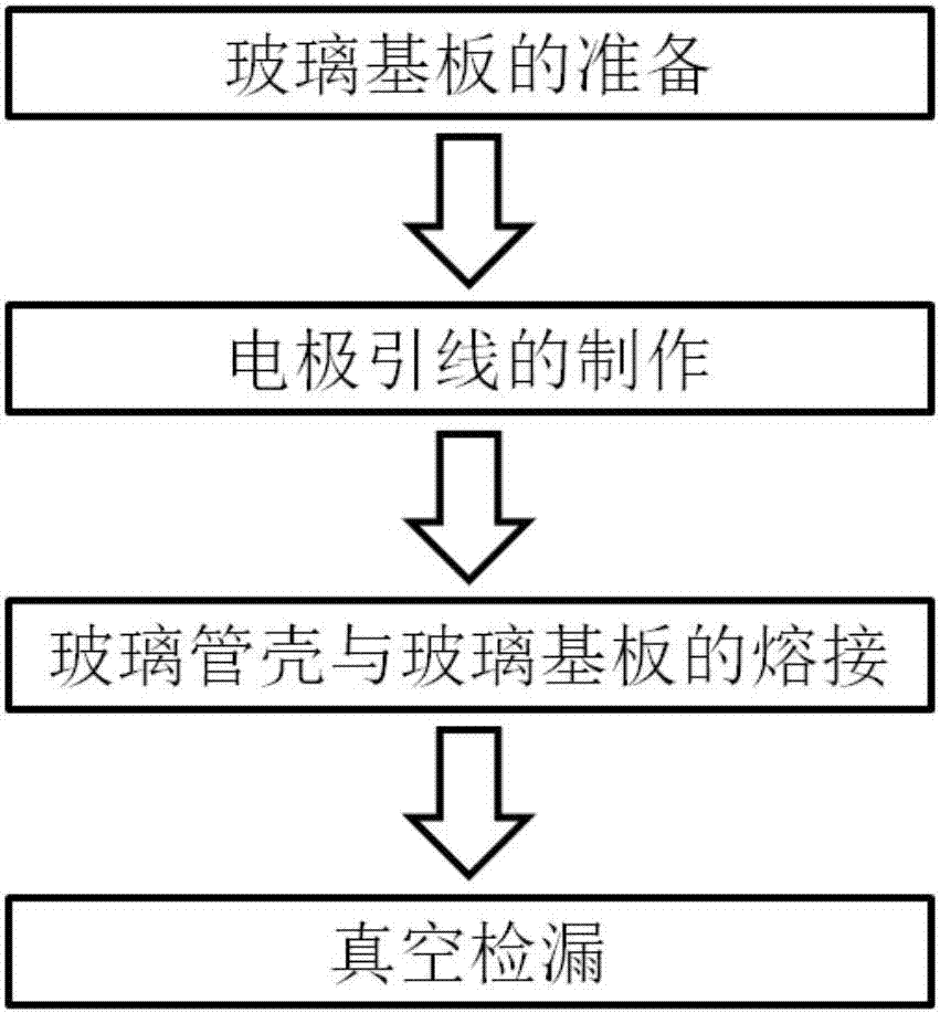
[0052] see figure 2 , the preferred implementation method of the present invention to make the electrode lead unit mainly includes the following steps:
[0053] First, the preparation of the glass substrate. Usually the glass substrate is made of borosilicate glass with a thickness of 2 mm and a flat surface. The size of the glass substrate is larger than 20 mm × 20 mm. It is ultrasonically cleaned with a glass cleaner and dried at high temperature.
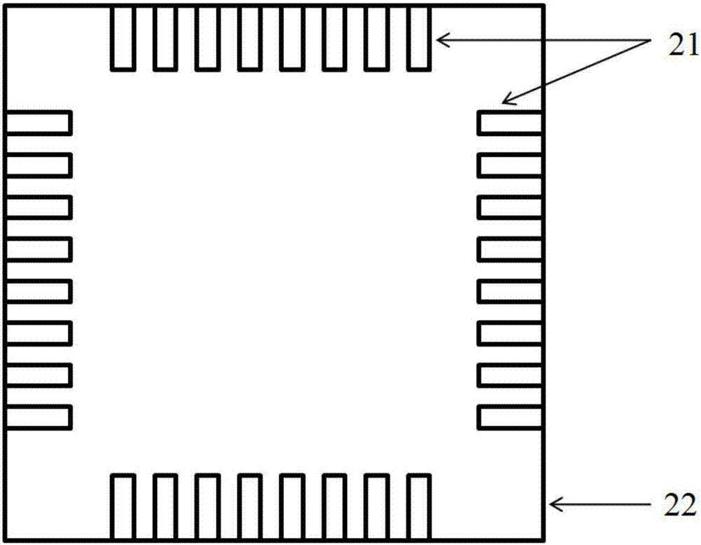
[0054] Second, the fabrication of electrode leads. Electrode leads are fabricated on glass substrates using standard semiconductor processes. The standard semiconductor process includes metal film deposition, photolithography, etching or corrosion or peeling, etc. The metal film can choose a single metal such as gold, silver or a stacked structure of multiple metal films such as titanium and platinum. The thickness of the metal film is greater than 500 nanometers. image 3 It is a typical electrode lead distribution state for...
PUM
 Abstract
Description
Claims
Application Information


