
Oxide semiconductor thin film and preparation process thereof

A technology of oxide semiconductor and preparation process, which is applied in the direction of semiconductor devices, transistors, electrical components, etc., can solve the problems of lower annealing temperature, high preparation cost, and non-environmental protection, and achieve low annealing temperature, lower process cost, and high anti-aging sexual effect

Inactive Publication Date: 2017-07-07
SOUTH CHINA UNIV OF TECH
View PDF9 Cites 7 Cited by
  • Summary
  • Abstract
  • Description
  • Claims
  • Application Information

AI Technical Summary

Problems solved by technology

However, this thin film is prepared by sputtering, which requires expensive vacuum equipment, and the preparation cost is high
[0009] Non-patent literature (Adv.Electron.Mater.2015,1,1500146) discloses a solution to prepare Sc, Y, La doped In 2 o 3 Thin film method, but this method uses organic solvents, and adds some flammable and explosive fuels to reduce the annealing temperature, which is not only not environmentally friendly, but also causes carbon residues

Method used


Image

  • Oxide semiconductor thin film and preparation process thereof
  • Oxide semiconductor thin film and preparation process thereof
  • Oxide semiconductor thin film and preparation process thereof

Examples


Embodiment 1

[0044] A kind of preparation technology of oxide semiconductor thin film, thin composition is M2x In 2-2x o 3-δ And the composition does not include Zn and Sn, where M is a group IIIB element in the periodic table of elements, 0.001≤x≤0.3, 0≤δ<3, the aqueous solution of In salt and M salt is used as the precursor solution for hydrolysis reaction, and then The solution after the hydrolysis reaction is formed into a film, and annealed at a temperature not higher than 300 degrees Celsius after the film is formed.

[0045] Group IIIB elements are one or any combination of two or more of Sc, Y, Ac, La, Ce, Pr, Nd, Pm, Sm, Eu, Gd, Tb, Dy, Ho, Er, Tm, Yb, or Lu Elements. It is preferably Nd or Sc, more preferably Sc.

[0046] The solute of the aqueous solution is one of nitrate, chloride, hydroxide or perchlorate. It is better for the solute of the aqueous solution to contain both nitrate and perchlorate.

[0047] The solute of the aqueous solution can also be at least two subst...

Embodiment 2

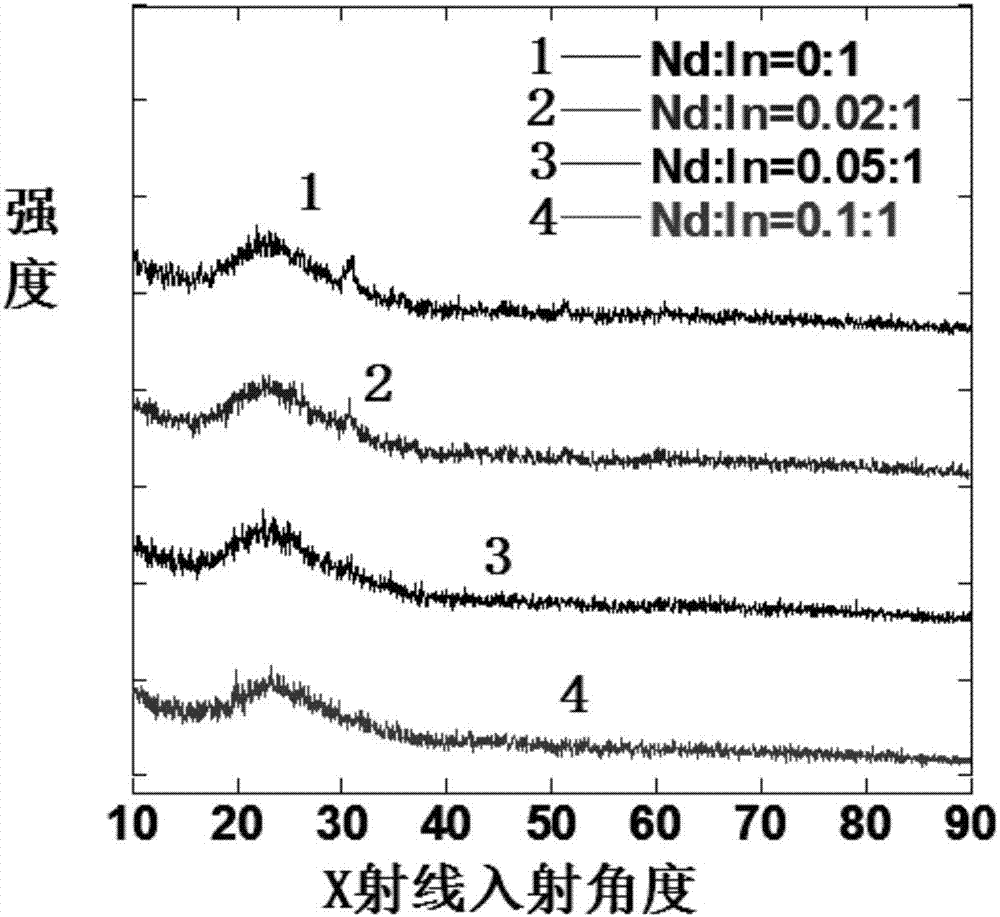
[0065] A method for preparing an oxide semiconductor film, the chemical formula of the composition of the oxide semiconductor film is expressed as Nd 2x In 2-2x o 3-δ , There are three options for x: 0.02, 0.05 and 0.1. The precursor solution is an aqueous solution of indium chloride and neodymium chloride, which is formed into a film by spin coating, followed by UV treatment, and then annealed at 180 degrees Celsius in an air atmosphere.

[0066] attached figure 1 Shows the different x prepared in this embodiment (x=0 represents undoped In 2 o 3 ) X-ray diffraction (XRD) pattern of the thin film, it can be seen that when the amount of Nd doped is small (x=0.02), In 2 o 3 The lattice structure of is well maintained, indicating that a small amount of Nd will not seriously damage the In 2 o 3 lattice structure. But when the amount of doped Nd is more (x≥0.05), In 2 o 3 The lattice damage is severe, mainly due to the Nd 3+ If the radius is too large, excessive doping ...

Embodiment 3

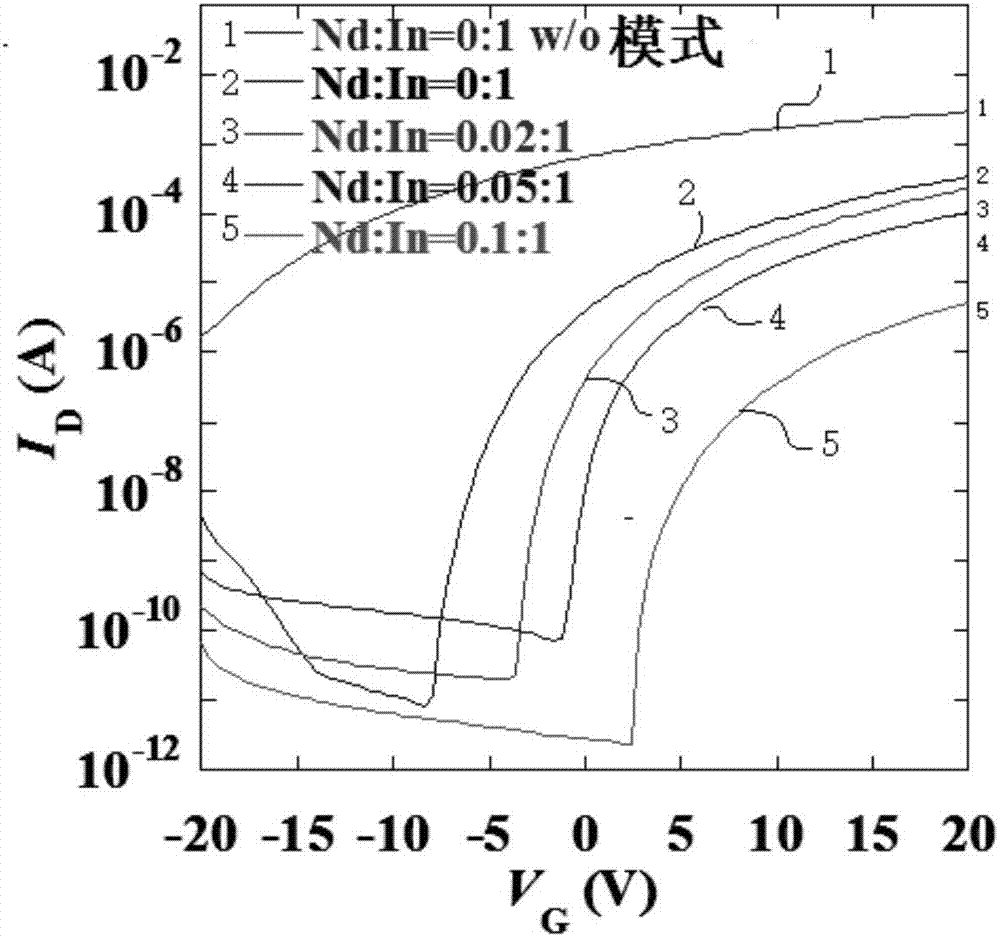
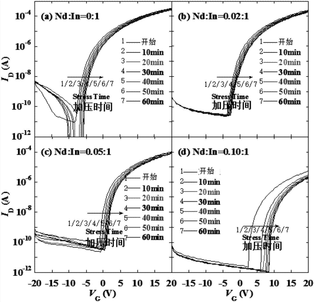
[0073] A preparation method of an oxide semiconductor thin film, the chemical formula of the composition is expressed as Sc 2x In 2-2x o 3-δ , There are three options for x: 0.02, 0.05 and 0.1. The precursor solution is an aqueous solution of indium nitrate and scandium nitrate, and the film is formed by spin coating, and the annealing temperature is 230 degrees Celsius.

[0074] attached Figure 4 Shows the different x prepared in this embodiment (x=0 represents undoped In 2 o 3 ) of the X-ray diffraction (XRD) pattern of the film, it can be seen that almost no In 2 o 3 The lattice structure of , which is mainly due to the Sc 3+ The radius of In 3+ The radii are similar and cause almost no lattice expansion.

[0075] The prepared thin film is used for the channel layer of the thin film transistor, with Figure 5The transfer characteristic curves of the aforementioned thin film transistors (TFTs) based on different Sc contents x are shown, and the performance paramet...


PUM


Abstract

The invention provides an oxide semiconductor thin film and a preparation process thereof. The ingredients of the thin film are M2xIn2-2xO3-delta, the ingredients do not contain Zn or Sn, M is a group IIIB element in a periodic table of elements, x is larger than or equal to 0.001 and smaller than or equal to 0.3, delta is larger than or equal to 0 and smaller than 3, the thin film is prepared with a water solution, and no carbon element is contained in the water solution. The water solution of In salt and M salt serves as a precursor solution for a hydrolysis reaction, the solution obtained after the hydrolysis reaction is subjected to film formation, and after film formation, the thin film is prepared after annealing at the temperature not higher than 300 DEG C. Solutes of the water solution are one of nitrate, chloride, hydroxide and perchlorate. The thin film prepared through the preparation method of the oxide semiconductor thin film has the high electron migration rate. The carrier concentration is adjusted by adjusting the content of the group IIIB element, and the thin film is good in turn-off performance, good in stability, simple in preparation process, high in adaptability and environmentally friendly.

Description

technical field [0001] The invention relates to the technical field of semiconductor materials and devices, in particular to an oxide semiconductor thin film and a preparation process thereof. Background technique [0002] In recent years, thin film transistors (TFT, Thin Film Transistor) based on oxide semiconductors have received more and more attention in the field of flat panel displays, especially in the field of organic electroluminescent displays (OLEDs). [0003] Currently, the semiconductor channel layer of thin film transistors used in flat panel displays is mainly made of silicon materials, including amorphous silicon (a-Si:H), polycrystalline silicon, and microcrystalline silicon. However, amorphous silicon thin film transistors are sensitive to light and have low mobility (<1cm 2 / Vs) and poor stability; although polysilicon thin film transistors have high mobility, their electrical uniformity is poor due to the influence of grain boundaries. In addition, du...

Claims


Application Information

Patent Timeline
Patent Type & Authority Applications(China)
IPC IPC(8): C03C17/23H01L29/786
CPCC03C17/23C03C2218/116H01L29/7869
Inventor 兰林锋王磊彭俊彪
Owner SOUTH CHINA UNIV OF TECH
Learn More