A kind of pin structure ultraviolet photodetector and preparation method thereof

A technology of electrical detectors and ultraviolet light, applied in circuits, electrical components, semiconductor devices, etc., can solve the problems of insensitivity of ultraviolet detectors and poor responsivity of weak ultraviolet signals, achieve high lateral carrier mobility, improve Effects of quantum efficiency and high absorption coefficient

Active Publication Date: 2018-07-06
苏州科帕特信息科技有限公司
View PDF7 Cites 2 Cited by
  • Summary
  • Abstract
  • Description
  • Claims
  • Application Information

AI Technical Summary

Problems solved by technology

[0005] Aiming at the defects of the prior art, the present invention provides a PIN structure ultraviolet photodetector, which solves the insensitivity of the ultraviolet detector caused by the similar ionization coefficients of electrons and holes in the AlGaN-based ultraviolet photodetector, and is sensitive to weak ultraviolet light. The problem of poor signal response

Method used


Image

  • A kind of pin structure ultraviolet photodetector and preparation method thereof

Examples


Embodiment 1

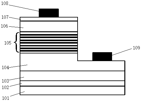
[0026] Example 1, such as figure 1 As shown, the PIN structure ultraviolet photodetector involved in this embodiment includes a sapphire substrate 101, an AlN nucleation layer 102, an Al x1 Ga 1-x1 N buffer layer 103, n-type Al x2 Ga 1-x2 N layer 104, non-doped i-type ZnO / TiO 2 Superlattice absorption layer 105, p-type Al x3 Ga 1-x3 N layer 106, p-type GaN layer 107, in n-type Al x2 Ga 1-x2 The n-type ohmic electrode 109 drawn out from the N layer 104 and the p-type ohmic electrode 108 drawn out on the p-type GaN layer 107 . The thickness of the AlN nucleation layer 102 is 25nm, and the specific thickness of the nucleation layer can be adjusted according to actual needs. Al x1 Ga 1-x1 The thickness of the N buffer layer 103 is 400 nm, and x1=0.30 therein. n-type Al x2 Ga 1-x2 The thickness of the N layer 104 is 700nm, and wherein x2=0.45, and is doped with Si, wherein the doping concentration of Si is greater than 5×10 18 cm -3 . Non-doped i-type ZnO / TiO 2 Sup...

Embodiment 2

[0038] Example 2, such as figure 1 As shown, the PIN structure ultraviolet photodetector involved in this embodiment includes a sapphire substrate 101, an AlN nucleation layer 102, an Al x1 Ga 1-x1 N buffer layer 103, n-type Al x2 Ga 1-x2 N layer 104, non-doped i-type ZnO / TiO 2 Superlattice absorption layer 105, p-type Al x3 Ga 1-x3 N layer 106, p-type GaN layer 107, in n-type Al x2 Ga 1-x2 The n-type ohmic electrode 109 drawn out from the N layer 104 and the p-type ohmic electrode 108 drawn out on the p-type GaN layer 107 . Wherein the thickness of the AlN nucleation layer 102 is 20 nm. al x1 Ga 1-x1 The thickness of the N buffer layer 103 is 300 nm, and x1=0.45 therein. n-type Al x2 Ga 1-x2 The thickness of the N layer 104 is 500nm, and wherein x2=0.55, and is doped with Si, wherein the doping concentration of Si is greater than 5×10 18 cm -3 . Non-doped i-type ZnO / TiO 2 Superlattice absorbing layer 105, ZnO layer thickness is 10nm in a single period, TiO 2...

Embodiment 3

[0040] Example 3, such as figure 1 As shown, the PIN structure ultraviolet photodetector involved in this embodiment includes a sapphire substrate 101, an AlN nucleation layer 102, an Al x1 Ga 1-x1 N buffer layer 103, n-type Al x2 Ga 1-x2 N layer 104, non-doped i-type ZnO / TiO 2 Superlattice absorption layer 105, p-type Al x3 Ga 1-x3 N layer 106, p-type GaN layer 107, in n-type Al x2 Ga 1-x2 The n-type ohmic electrode 109 drawn out from the N layer 104 and the p-type ohmic electrode 108 drawn out on the p-type GaN layer 107 . Wherein the thickness of the AlN nucleation layer 102 is 60nm. al x1 Ga 1-x1 The thickness of the N buffer layer 103 is 800 nm, and x1=0.4 therein. n-type Al x2 Ga 1-x2 The thickness of the N layer 104 is 1000 nm, and wherein x2=0.6, and is doped with Si, wherein the doping concentration of Si is greater than 5×10 18 cm -3 . Non-doped i-type ZnO / TiO 2 Superlattice absorbing layer 105, ZnO layer thickness is 10nm in a single period, TiO 2 ...


PUM


Abstract

The invention discloses a PIN structure ultraviolet photoelectric detector. The PIN structure ultraviolet photoelectric detector comprises a sapphire substrate, an AIN nucleation layer, an Alx1Gal-x1N buffer layer, an n-type Alx2Gal-x2N layer, a non-doped i-type ZnO / TiO2 superlattice absorption layer, a p-type Alx3Gal- x3N layer, and a p-type GaN layer. An n-type ohmic electrode is led out from the n-type Alx2Gal-x2N layer, and a p-type ohmic electrode is led out from the p-type GaN layer. In the non-doped i-type ZnO / TiO2 superlattice absorption layer, the repetition period of the superlattice is in a range from 1 to 10. The invention also discloses the preparation method of the PIN structure ultraviolet photoelectric detector. By using the PIN structure ultraviolet photoelectric detector, the responsivity of the detector to weak ultraviolet signals is improved.

Description

technical field [0001] The invention relates to an ultraviolet photodetector and a preparation method thereof, in particular to a PIN structure ultraviolet photodetector and a preparation method thereof, and belongs to the field of semiconductor optoelectronic devices. Background technique [0002] Ultraviolet photodetectors have important application value and development prospects in both military and civilian applications, such as: ultraviolet warning and guidance, detection of hydrocarbon combustion flames, detection of biochemical genes, research in ultraviolet astronomy, short-distance communication and skin disease treatment, etc. The PIN structure ultraviolet photodetector has the advantages of small size, light weight, long life, good shock resistance, low working voltage, high temperature resistance, corrosion resistance, radiation resistance, high quantum efficiency and no need for filters. research hotspots. [0003] GaN-based semiconductor ternary compound Al ...

Claims


Application Information

Patent Timeline
Patent Type & Authority Patents(China)
IPC IPC(8): H01L31/0296H01L31/032H01L31/0352H01L31/105H01L31/18
CPCH01L31/0296H01L31/032H01L31/035236H01L31/105H01L31/18H01L31/1836H01L31/1848H01L31/1852Y02P70/50
Inventor 王书昶刘玉申李中国冯金福
Owner 苏州科帕特信息科技有限公司
Why Eureka
Try Eureka