High-resistance cap layer-based III-nitride polarization super-junction high electron mobility transistor (HEMT) device and fabrication method thereof

A technology of capping layer and nitride, which is applied in semiconductor/solid-state device manufacturing, semiconductor devices, electrical components, etc., can solve the problems of reducing the concentration of two-dimensional electron gas and low current density of polarized superjunction devices, so as to avoid etching damage, compensate for low current density, and increase the effect of current density

Inactive Publication Date: 2017-07-25
SUZHOU NENGWU ELECTRONICS TECH
View PDF4 Cites 24 Cited by
  • Summary
  • Abstract
  • Description
  • Claims
  • Application Information

AI Technical Summary

Problems solved by technology

The damage caused by excessive etching process and the polarized superjunction structure reduce the concentration of part of the two-dimensional electron gas, so the current density of the traditional enhanced polarized superjunction device is very low

Method used


Image

  • High-resistance cap layer-based III-nitride polarization super-junction high electron mobility transistor (HEMT) device and fabrication method thereof
  • High-resistance cap layer-based III-nitride polarization super-junction high electron mobility transistor (HEMT) device and fabrication method thereof
  • High-resistance cap layer-based III-nitride polarization super-junction high electron mobility transistor (HEMT) device and fabrication method thereof

Examples


Embodiment 1

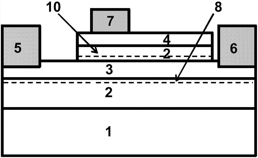
[0109] Example 1: Please see again image 3 and Image 6 In a typical implementation involved in this embodiment, a method for fabricating a polarized superjunction enhanced HEMT realized by using a high-resistance capping layer and a p-type gate technology includes the following steps:

[0110] (1) Treat the substrate surface in the reaction chamber of the epitaxial growth equipment;

[0111] (2) Epitaxial growth of AlGaN / GaN epitaxial layer and p-GaN on the substrate, wherein the thickness of GaN is 1μm-8μm, the thickness of AlGaN is 14nm-30nm, and the molar content of Al element is 15%-30%, p -GaN thickness is 50-110nm, Mg doping concentration is 10 19 After being taken out from the chamber, it is cleaned with an organic solution and purged with high-purity nitrogen;

[0112] (3) Perform photolithography and development on the cleaned device, the photoresist is AZ5214, the exposure time is 6.5s, the development time is 50s-60s, and the table is isolated, and ion implanta...

Embodiment 2

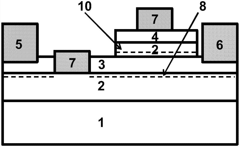
[0117] see again image 3 and Figure 7 In a typical implementation that this embodiment relates to, the method for making a polarized superjunction enhanced HEMT that adopts a high-resistance capping layer and a p-type gate technology includes the following steps:

[0118] (1) processing the substrate surface in the reaction chamber;

[0119](2) Epitaxial growth of AlGaN / GaN epitaxial layer and Mg-doped non-activated high-resistance GaN on the substrate, wherein the thickness of GaN is 1 μm-8 μm, the thickness of AlGaN is 14nm-30nm, and the molar content of Al element is 15 %-30%, the thickness of high-resistance GaN is 50-110nm, and the Mg doping concentration is 10 19 After being taken out from the chamber, it is cleaned with an organic solution and purged with high-purity nitrogen;

[0120] (3) Perform photolithographic development on the cleaned device, the photoresist is AZ5214, the exposure time is 6.5s, the development time is 50s-60s, and the table is isolated, and...


PUM


Abstract

The invention discloses a high-resistance cap layer-based III-nitride polarization super-junction high electron mobility transistor (HEMT) device and a fabrication method thereof. The device comprises a first heterojunction, a second heterojunction, a p-type doping fourth semiconductor, a source, a drain and a gate, wherein the first heterojunction comprises a first semiconductor and a second semiconductor, the second semiconductor is formed on the first semiconductor and is provided with a band gap wider than the first semiconductor, a two-dimensional electron gas is formed in a first heterojunction structure, the second heterojunction comprises the second semiconductor and a third semiconductor, the third semiconductor is formed on the second semiconductor and is provided with a band gap narrower than the second semiconductor, a two-dimensional electron gas is formed in a second heterojunction structure, the fourth semiconductor is formed on the second semiconductor, the fourth semiconductor and the third semiconductor are closely connected in a horizontal direction, the source and the drain are connected with the first heterojunction and can be electrically connected through the two-dimensional electron gases, and the gate is arranged between the source and the drain and is connected with the fourth semiconductor.

Description

technical field [0001] The present invention relates to a polarized superjunction HEMT (high electron mobility transistor) device and a manufacturing method thereof, in particular to a III-nitride polarized superjunction HEMT device based on a high-resistance capping layer and a manufacturing method thereof, belonging to power semiconductor technology field. Background technique [0002] Group III nitrides (such as GaN) have the advantages of large band gap, high electron mobility, high breakdown field strength, etc., which can meet the requirements of higher power, higher frequency, smaller volume and higher power devices in the next generation of power electronic systems. Due to the requirement of high temperature work, HEMT devices made of group III nitrides (such as AlGaN / GaN HEMTs) have become a hot spot in the research of new generation power devices. However, currently III-nitride HEMTs still face many problems, such as current collapse, low breakdown voltage, and en...

Claims


Application Information

Patent Timeline
Patent Type & Authority Applications(China)
IPC IPC(8): H01L29/778H01L21/335
CPCH01L29/7783H01L29/66462
Inventor 郝荣晖付凯于国浩蔡勇张宝顺
Owner SUZHOU NENGWU ELECTRONICS TECH
Why Eureka
Try Eureka