Method and device for precisely and controllably cutting graphene bands through photo-catalytic oxidation function

A photocatalytic oxidation and graphene ribbon technology, applied in metal processing and other directions, can solve problems such as human injury, equipment corrosion, and rough graphene edges, and achieve the effect of avoiding equipment corrosion.

Active Publication Date: 2017-07-28
SHENYANG POLYTECHNIC UNIV
View PDF6 Cites 6 Cited by
  • Summary
  • Abstract
  • Description
  • Claims
  • Application Information

AI Technical Summary

Problems solved by technology

[0006] The present invention solves the problem of extremely high width and edge structure requirements of graphene ribbons in the field of electronics, and the difficulty in achieving controllable and smooth edge cutting of graphene in current manufacturing methods. The traditional AFM probe scribing technology has problems such as warped and rough edges of graphene caused by excessive mechanical action. A new method and device for precise and controllable cutting of graphene using photocatalytic excitation of chemical shears is proposed.
It solves the problems of equipment corrosion, environmental pollution, human injury, and easy failure caused by the use of traditional strengthening reagents, as well as the problems of expensive equipment, complicated operating conditions, and difficult control caused by plasma and transition metals.

Method used


Image

  • Method and device for precisely and controllably cutting graphene bands through photo-catalytic oxidation function
  • Method and device for precisely and controllably cutting graphene bands through photo-catalytic oxidation function
  • Method and device for precisely and controllably cutting graphene bands through photo-catalytic oxidation function

Examples


Embodiment 1

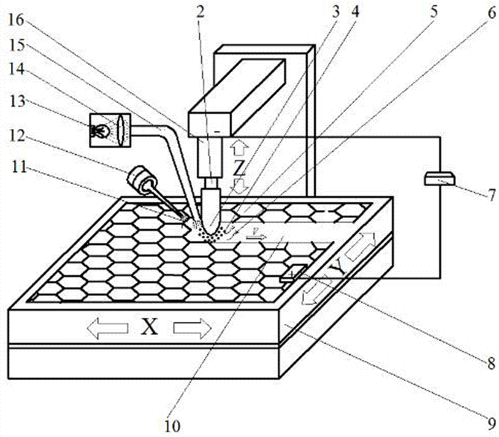
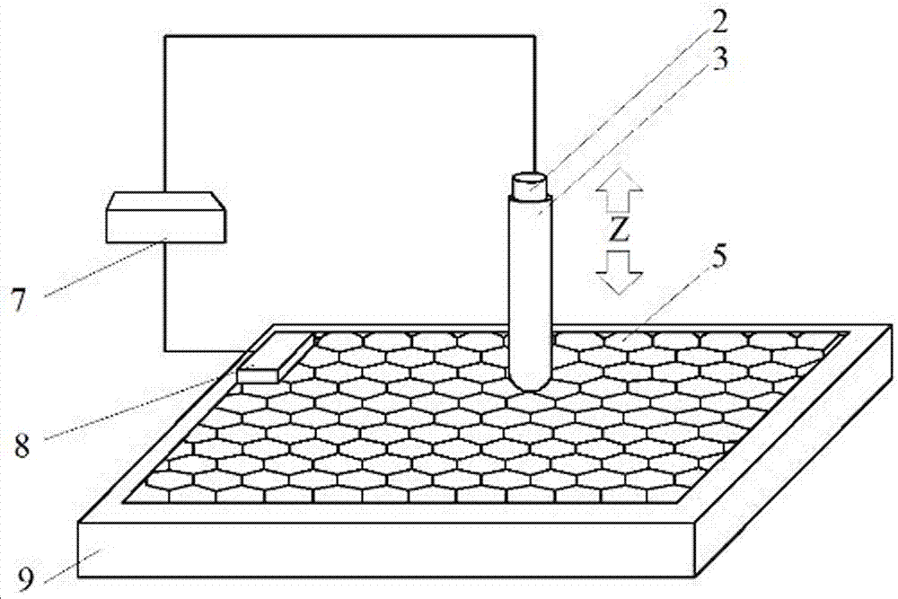
[0037] Step 1: fixing the graphene 5 with the substrate on the two-dimensional micro-motion stage 9 driven by piezoelectric ceramics, the two-dimensional micro-motion stage 9 is nanoscale;

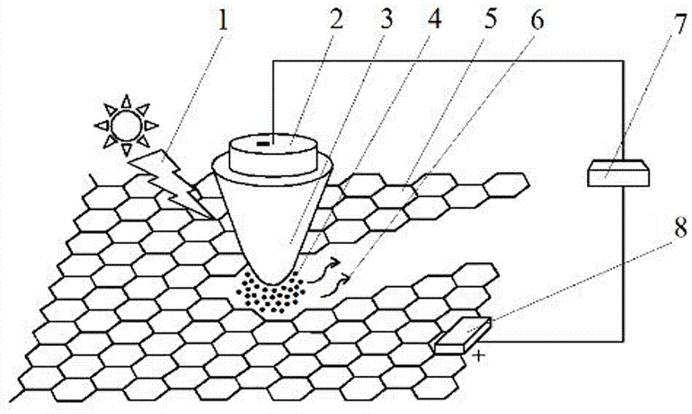
[0038] Step 2: Use the magnetostrictive mechanism 16 and the power controller 7 to realize the Z-direction positioning of the semiconductor probe 3. The material of the outer layer of the semiconductor probe 3 is titanium dioxide, the material of the metal core 2 of the inner layer is titanium, and the outer layer of the semiconductor probe 3 is titanium dioxide. The diameter size is 20nm, and the lower end is smoothly transitioned;

[0039] Step 3: Use atomizer 12 to make the mass percentage 0.5%H 2 o 2 The auxiliary liquid 11 mixed with 99.5% deionized water is atomized, and the atomized auxiliary liquid 11 is adsorbed on the surface of the semiconductor probe 3;

[0040] Step 4: The ultraviolet light source 13 emits ultraviolet light 1, which is focused by the condenser lens 14 and ir...

Embodiment 2

[0045] Step 1: fixing the graphene 5 with the substrate on the two-dimensional micro-motion stage 9 driven by piezoelectric ceramics, the two-dimensional micro-motion stage 9 is nanoscale;

[0046] Step 2: Use the magnetostrictive mechanism 16 and the power controller 7 to realize the Z-direction positioning of the semiconductor probe 3. The material of the outer layer of the semiconductor probe 3 is zinc oxide, the material of the metal core 2 of the inner layer is zinc, and the material of the semiconductor probe 3 is zinc oxide. The outer diameter is 50nm, with a smooth transition at the lower end;

[0047] Step 3: use the atomizer 12 to atomize the auxiliary liquid 11 formed by mixing 1% Fenton reagent and 99% deionized water by mass percentage, and the atomized auxiliary liquid 11 is adsorbed on the surface of the semiconductor probe 3;

[0048] Step 4: The ultraviolet light source 13 emits ultraviolet light 1, which is focused by the condenser lens 14 and irradiated on t...

Embodiment 3

[0053] Step 1: fixing the graphene 5 with the substrate on the two-dimensional micro-motion stage 9 driven by piezoelectric ceramics, the two-dimensional micro-motion stage 9 is nanoscale;

[0054] Step 2: Use the magnetostrictive mechanism 16 and the power controller 7 to realize the Z-direction positioning of the semiconductor probe 3. The material of the outer layer of the semiconductor probe 3 is zirconium dioxide, and the material of the metal core 2 of the inner layer is zirconium. 3 The outer diameter is 100nm, and the lower end is smoothly transitioned;

[0055] Step 3: Use atomizer 12 to make the mass percentage 12%K 2 FeO 4 The auxiliary liquid 11 mixed with 88% deionized water is atomized, and the atomized auxiliary liquid 11 is adsorbed on the surface of the semiconductor probe 3;

[0056] Step 4: The ultraviolet light source 13 emits ultraviolet light 1, which is focused by the condenser lens 14 and irradiated on the semiconductor probe 3 by the light source tra...


PUM


Abstract

The invention relates to a method and device for precisely and controllably cutting graphene bands through a photo-catalytic oxidation function. The method is characterized by comprising the steps that firstly, graphene with a substrate is fixed to a two-dimensional micromotion platform driven by piezoelectric ceramic; secondly, Z-direction locating of a semiconductor probe is achieved through a magnetostriction mechanism with the help of a power controller; thirdly, an atomizer is used for atomizing auxiliary liquid, and the atomized auxiliary liquid is adsorbed to the surface of the semiconductor probe; and fourthly, an ultraviolet source emits ultraviolet light, the ultraviolet light irradiates the semiconductor probe through a light source transmission device after being focused through a collecting lens, and meanwhile through combination of ultraprecise motion of the two-dimensional micromotion platform in the direction X and the direction Y, the graphene bands with different two-dimensional patterns are cut. By means of the method and device, the problems of equipment corrosion, environment pollution, human body hurt and easy failing caused by using a traditional enhancement reagent and the problems of expensive equipment, complex operation conditions, control difficulty and the like caused by plasma and transition metal are solved.

Description

technical field [0001] The invention belongs to the field of ultra-precision cutting and processing, and relates to a method and a device for precisely and controllably cutting graphene ribbons by using photocatalytic oxidation. Background technique [0002] Graphene is made of carbon atoms with sp ²The hexagonal honeycomb lattice planar film composed of hybrid orbital connections is a new two-dimensional material with a thickness of only one carbon atom, and is the basic unit for constructing all other dimensional graphite materials. Graphene not only has extraordinary electrical properties (electron mobility at room temperature can reach 2×10 5 cm 2 / (V s), which is tens to hundreds of times that of traditional semiconductor materials), outstanding specific surface area (2630m 2 / g), excellent thermal conductivity (5000 W / (m K)), and also has some unique properties, such as a series of properties such as perfect quantum tunneling effect and never-disappearing electrical...

Claims


Application Information

Patent Timeline
Patent Type & Authority Applications(China)
IPC IPC(8): B26F3/16B26D7/00
CPCB26D7/00B26D2007/0012B26F3/16
Inventor 苑泽伟何艳郑鹏韩晖
Owner SHENYANG POLYTECHNIC UNIV
Why Eureka
Try Eureka