A kind of organic light-emitting display panel and preparation method thereof

A light-emitting display, organic light-emitting device technology, applied in semiconductor/solid-state device manufacturing, coating, electric solid device and other directions, can solve the problems of weak adhesion, unfavorable device bending, thick inorganic layer, etc., to achieve good elasticity and toughness, Good seismic performance and surface can resist the effect

Active Publication Date: 2019-06-18
WUHAN TIANMA MICRO ELECTRONICS CO LTD +1
View PDF10 Cites 0 Cited by
  • Summary
  • Abstract
  • Description
  • Claims
  • Application Information

AI Technical Summary

Problems solved by technology

As far as the current thin film packaging technology is concerned, there are still the following problems to be solved: ① The inorganic layer is relatively thick, which is not conducive to device bending, and the current inorganic layer manufacturing process is prone to defects and particles, which is not conducive to blocking water and oxygen; The performance of organic matter (acrylic) needs to be improved, such as UV shrinkage, outgassing, thermal expansion (CTE), yellowing, etc.; Shedding occurs; ④Acrylic materials are easy to absorb water and have strict requirements on the process environment

Method used


Image

  • A kind of organic light-emitting display panel and preparation method thereof
  • A kind of organic light-emitting display panel and preparation method thereof
  • A kind of organic light-emitting display panel and preparation method thereof

Examples


preparation example Construction

[0105] The preparation method of the inorganic barrier layer may illustratively include any one of sputtering, chemical vapor deposition, metal-organic chemical vapor deposition, plasma chemical vapor deposition, atomic evaporation, and electron cyclotron resonance.

[0106] In a specific embodiment, the material of the inorganic encapsulation layer is silicon nitride or aluminum oxide.

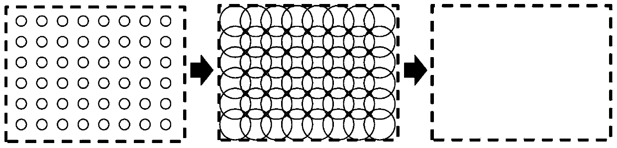
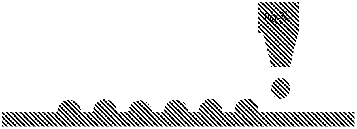
[0107] In a specific embodiment, the organic encapsulation layer is formed by inkjet printing.

[0108] The present invention also provides a method for preparing an organic light-emitting display panel, the method comprising the following steps:

[0109] Provide the substrate;

[0110] forming an organic light emitting device on the substrate;

[0111] An encapsulation layer is formed on the side of the organic light-emitting device away from the substrate, the encapsulation layer includes at least one organic encapsulation layer, and the organic encapsulation layer is obtained by cross-li...

Embodiment 1

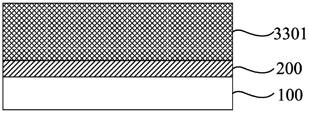
[0119] A kind of organic light-emitting display panel (structure such as image 3 shown), including a silicon substrate, an organic light emitting device (OLED) 200 disposed on one side of the silicon substrate 100, and an encapsulation layer covering the OLED 200, the encapsulation layer is a first organic encapsulation layer 3301, and the organic encapsulation layer Layer 300 is a polymer with a network structure obtained by crosslinking polyorganosiloxane;

[0120] The raw materials of the polymer with network structure obtained by polyorganosiloxane crosslinking include:

[0121] (i) blocks have The structure of polyorganosiloxane, the degree of polymerization is 20, The siloxane unit accounts for 80% of the total number of polysiloxane siloxane repeating units; 50 parts by weight;

[0122] (ii) The block has The structure of polyorganosiloxane, the degree of polymerization is 20, The siloxane unit accounts for 80% of the total number of polysiloxane siloxane repe...

Embodiment 2

[0130] The difference from Example 1 is that the raw materials of the polymer with a network structure obtained by crosslinking polyorganosiloxane include:

[0131] (i) blocks have The structure of polyorganosiloxane, the degree of polymerization is 20, The siloxane unit accounts for 80% of the total number of polysiloxane siloxane repeating units; 80 parts by weight;

[0132] (ii) The block has The structure of polyorganosiloxane, the degree of polymerization is 20, The siloxane unit accounts for 80% of the total number of polysiloxane siloxane repeating units; 15 parts by weight;

[0133] (iii) 2,4,6-trichloro-s-triazine, 5 parts by weight.


PUM

PropertyMeasurementUnit
thicknessaaaaaaaaaa
thicknessaaaaaaaaaa
wavelengthaaaaaaaaaa

Abstract

The present invention relates to an organic light-emitting display panel, which is characterized in that it comprises a substrate; an organic light-emitting device is arranged on one side of the substrate; an encapsulation layer is arranged on a side of the organic light-emitting device away from the substrate, and The encapsulation layer includes at least one organic encapsulation layer; wherein, at least one organic encapsulation layer is formed of a polymer with a network structure obtained by crosslinking polyorganosiloxane. The present invention selects the network structure obtained by polyorganosiloxane cross-linking as the material of the organic encapsulation layer, has high light transmittance (more than 98%), can realize photocuring, good shock resistance, surface energy resistance, temperature change resistance, and anti-corrosion. Advantages of yellowing.

Description

technical field [0001] The invention belongs to the field of display panel design, and in particular relates to an organic light emitting display panel and a preparation method thereof, in particular to an organic light emitting display panel including a specific encapsulation layer and a preparation method thereof. Background technique [0002] Thin film encapsulation (TFE) can encapsulate OLEDs on rigid substrates or flexible substrates (plastic substrates, such as PEN, PES, PC, PET), especially OLEDs on flexible substrates, which can realize the bendability and rollability of flexible OLEDs sex. [0003] Existing thin-film packaging structures mostly use inorganic / organic stacking structures to package OLED devices, with 3 layers, 5 layers, or even more layers. Among them, the inorganic layer mainly plays the role of blocking water and oxygen erosion, while the organic layer has the following functions: [0004] ①Planarization: covering particles and TFT substrate steps...

Claims


Application Information

Patent Timeline
Patent Type & Authority Patents(China)
IPC IPC(8): H01L51/52H01L51/56
CPCH10K50/844H10K71/00C09D183/04C09D183/08C08G77/20C08G77/28
Inventor 金健苏聪艺
Owner WUHAN TIANMA MICRO ELECTRONICS CO LTD
Why Eureka
Try Eureka