Preparation method of exposing high-energy (001) crystal face ultrathin CdS nanobelt

A nanobelt and ultra-thin technology, applied in the field of photocatalysis, can solve the problems that are not conducive to large-scale industrial production, high equipment requirements, high reaction temperature, etc., and achieve the effect of inhibiting the probability of bulk phase recombination, low reaction temperature and good repeatability

Inactive Publication Date: 2017-08-29
XIANGTAN UNIV
View PDF3 Cites 0 Cited by
  • Summary
  • Abstract
  • Description
  • Claims
  • Application Information

AI Technical Summary

Problems solved by technology

In these synthetic methods, the reaction temperature is higher than 180°C. Higher reaction temperature requires high equipment and increases energy consumption, which is not conducive to large-scale industrial production.

Method used


Image

  • Preparation method of exposing high-energy (001) crystal face ultrathin CdS nanobelt
  • Preparation method of exposing high-energy (001) crystal face ultrathin CdS nanobelt
  • Preparation method of exposing high-energy (001) crystal face ultrathin CdS nanobelt

Examples


Embodiment 1

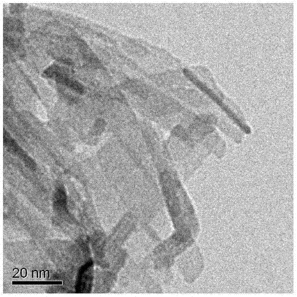
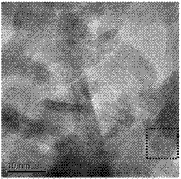
[0023] 10.0mmol Cd(NO 3 ) 2 , 33.4mmol S powder, 5.0mmol deionized, 1000.0mmol diethylenetriamine were fully stirred and dispersed evenly, and then placed in a 120ml polytetrafluoroethylene reactor, at a reaction temperature of 60°C and a stirring rate of 600 rpm Next, solvothermal reaction for 72h. After natural cooling to room temperature, the solvothermal product was collected by centrifugation. Then the product was dispersed in deionized water, the pH value of the solution was adjusted to 8, and ultrasonic stripping was performed for 10 h to obtain ultrathin CdS nanobelts with exposed high-energy (001) crystal planes. The thickness of the CdS nanobelt is about 1nm, the width is about 5nm, and the length is about 100nm as measured by an atomic force microscope.

Embodiment 2

[0025] 1.7mmol CdCl 2 2.5H 2 O, 15.0mmol S powder, 1.0mmol deionized, 1000.0mmol diethylenetriamine were fully stirred and dispersed evenly, and then placed in a 120ml polytetrafluoroethylene reactor, at a reaction temperature of 80°C and a stirring rate of 300 rpm Conditions, solvothermal reaction 48h. After natural cooling to room temperature, the solvothermal product was collected by centrifugation. Then the product was dispersed in deionized water, the pH value of the solution was adjusted to 9.0, and the ultrathin CdS nanoribbons with exposed high-energy (001) crystal planes were obtained by ultrasonic stripping for 2 h. The thickness of the CdS nanobelt is about 1nm, the width is about 10nm, and the length is about 100nm as measured by an atomic force microscope.

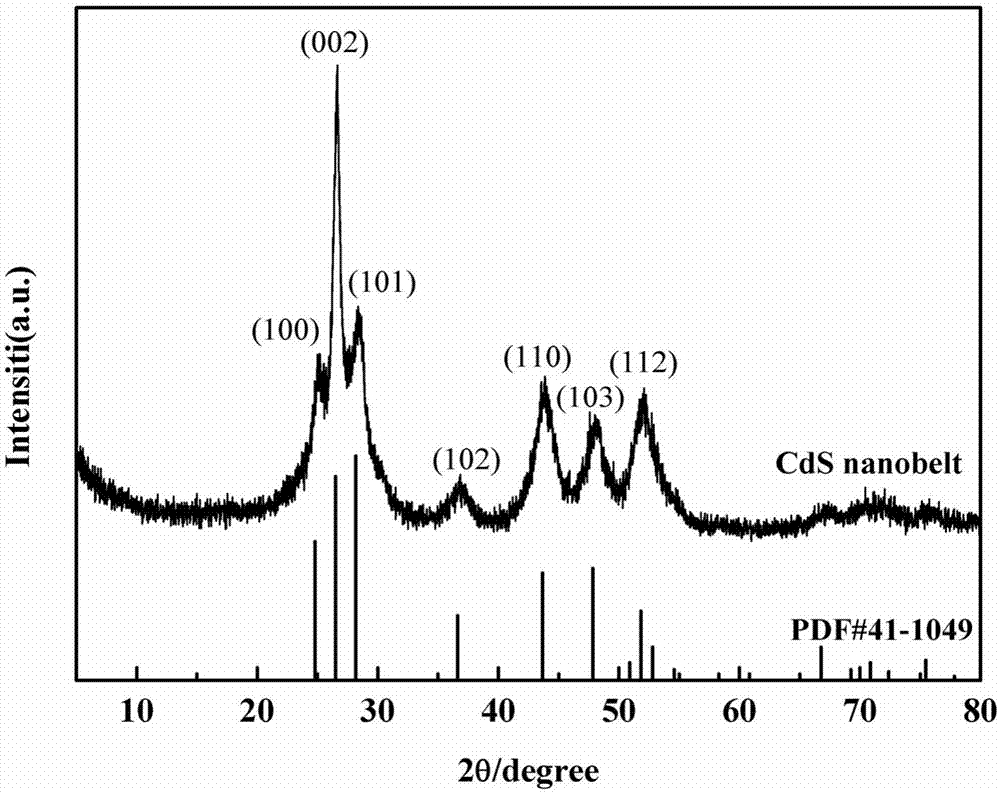
[0026] Such as figure 1 As shown, the (002) and (101) crystal plane diffraction peak intensity difference of CdS semiconductor standard PDF card is not big, and the (001) crystal plane diffraction peak int...

Embodiment 3

[0035] 3.0mmol CdCl 2 , 1.0mmol Cd(CH 3 COO) 2 , 5.0mmol S powder, 3.0mmol deionized, 1000.0mmol diethylenetriamine were fully stirred and dispersed evenly, and then placed in a 120ml polytetrafluoroethylene reactor, under the conditions of a reaction temperature of 100°C and a stirring rate of 30 rpm Next, solvothermal reaction for 72h. After natural cooling to room temperature, the solvothermal product was collected by centrifugation. Then the product was dispersed in deionized water, the pH value of the solution was adjusted to 10.5, and the ultrathin CdS nanoribbons with exposed high-energy (001) crystal planes were obtained by ultrasonic stripping for 6 h. The thickness of the nanobelt is about 3nm, the width is about 15nm, and the length is about 100nm as measured by an atomic force microscope.


PUM

PropertyMeasurementUnit
thicknessaaaaaaaaaa
widthaaaaaaaaaa
lengthaaaaaaaaaa

Abstract

The invention discloses a preparation method of an exposing high-energy (001) crystal face ultrathin CdS nanobelt. The preparation method comprises the following steps: 1) uniformly mixing inorganic cadmium salt, deionized water, diethylenetriamine and sulfur powder, performing a solvent thermal response while a mixture is stirred to obtain a solvent heat product; and 2) dispersing the solvent heat product in deionized water, performing ultrasonic peeling to obtain the exposing high-energy (001) crystal face ultrathin CdS nanobelt. The method comprises the following technical effects that 1) the prepared CdS nanobelt mainly expose the (001) high-energy crystal face, has the characteristics of electronic orientation transmission, fast transmission rate and special optical performance; and 2) the thickness of the CdS nanobelt is thin, specific surface area is enlarged, migration distance between photogenerated charge and the surface of a catalyst is greatly shortened, composite probability of photogenerated charge and cavity on a generation body can be effectively inhibited; 3) under visible light irradiation with wavelength being greater than 420 nm and condition of no loading of a cocatalyst , hydrogen production efficiency of the CdS nanobelt can reach as high as 59.7 mmol/h/g, illumination is carried out for 50 h, and the catalytic activity has no obvious reduction; and 4) the method has the advantages of simple operation, low reaction temperature and good repeatability.

Description

technical field [0001] The invention belongs to the technical field of photocatalysis, and in particular relates to a method for preparing ultra-thin CdS nanobelts with exposed high-energy (001) crystal planes. Background technique [0002] CdS is a semiconductor photocatalytic material with a narrow band gap and excellent visible light response characteristics. It has two crystal structures of hexagonal wurtzite and cubic sphalerite. Due to its unique optical, electrical and catalytic properties, it is widely used in the fields of solar cells, light-emitting diodes, lasers and catalysis. [0003] Since Professor Wang Zhonglin reported ZnO nanoribbons in 2001, one-dimensional nanoribbon materials have attracted widespread attention due to their properties such as directional electron transport, large aspect ratio, and anisotropy. At present, the preparation method of CdS nanobelts is commonly used by chemical vapor deposition (Nanotechnology, 2011, 22 (13): 135702; Advanced...

Claims


Application Information

Patent Timeline
Patent Type & Authority Applications(China)
IPC IPC(8): C01G11/02B82Y40/00B01J27/04C01B3/04
CPCB01J27/04B01J35/004B82Y40/00C01B3/042C01G11/02C01P2002/72C01P2004/04C01P2004/17C01P2004/64C01P2006/60Y02E60/36
Inventor 赵才贤陈烽张立群詹夏易兰花罗和安
Owner XIANGTAN UNIV
Why Eureka
Try Eureka