
CdZnTe planar detector surface treatment method

A surface treatment and detector technology, applied in the field of planar detector surface treatment, can solve problems such as poor energy resolution, achieve the effects of improving stoichiometric ratio, reducing leakage current, and reducing scattering

Inactive Publication Date: 2017-09-01
NORTHWESTERN POLYTECHNICAL UNIV
View PDF4 Cites 14 Cited by
  • Summary
  • Abstract
  • Description
  • Claims
  • Application Information

AI Technical Summary

Problems solved by technology

[0009] In order to overcome the deficiency of poor energy resolution of the planar detector after the existing planar detector surface treatment method, the present invention provides a CdZnTe planar detector surface treatment method

Method used


Image

  • CdZnTe planar detector surface treatment method
  • CdZnTe planar detector surface treatment method
  • CdZnTe planar detector surface treatment method

Examples


Embodiment 1

[0028] Step 1. Make the size 5×5×2mm 3 The CZT wafer is first rough polished on both sides with MgO on the grinding and polishing machine, and then polished with fine polishing liquid.

[0029] Step 2. After cleaning and drying the polished CZT wafer, configure a bromomethanol etching solution with a concentration of 1:50, etch the CZT wafer in the bromomethanol etching solution for 2 minutes, and then wash and dry it with deionized water after etching. This step was done in a fume hood.

[0030] Step 3, plate Au electrodes on the corroded CZT wafer within half an hour by vacuum evaporation method, and vacuumize 5×10 -3 After Pa, vapor-deposit on both sides for 5 minutes.

[0031] Step 4. Protect the Au electrode surface with photoresist, remove the side damage layer by side polishing, then passivate the side with hydrogen peroxide for 5 minutes, and finally remove the photoresist with acetone, clean the CZT wafer and dry it to obtain a CZT planar detector .

[0032] Step ...

Embodiment 2

[0038] Step 1. Make the size 5×5×2mm 3 The CZT wafer is first rough polished with MgO on both sides on the grinding and polishing machine, and then polished with fine polishing liquid.

[0039] Step 2. After the polished CZT wafer was cleaned and dried, a bromomethanol etching solution with a concentration of 1:50 was prepared, and the CZT wafer was statically etched in the bromomethanol etching solution for 3 minutes. After etching, it was cleaned with deionized water and dried. This step was done in a fume hood.

[0040] Step 3. Plating Au electrodes on the corroded CZT wafer within half an hour by vacuum evaporation method, vacuuming 5×10 -3 After Pa, vapor-deposit on both sides for 4 minutes.

[0041] Step 4. Protect the Au electrode surface with photoresist, remove the side damage layer by side polishing, then passivate the side with hydrogen peroxide for 8 minutes, and finally remove the photoresist with acetone, clean the CZT wafer and dry it to obtain a CZT planar de...

Embodiment 3

[0047] Step 1. Make the size 5×5×2mm 3 The CZT wafer is first rough polished with MgO on both sides on the grinding and polishing machine, and then polished with fine polishing liquid.

[0048] Step 2. After cleaning and drying the polished CZT wafer, configure a bromomethanol etching solution with a concentration of 1:50, etch the CZT wafer in the bromomethanol etching solution for 5 minutes, and then wash and dry the CZT wafer with deionized water after etching. This step was done in a fume hood.

[0049] Step 3. Plating Au electrodes on the corroded CZT wafer within half an hour by vacuum evaporation method, vacuuming 5×10 -3 After Pa, vapor-deposit on both sides for 3 minutes.

[0050] Step 4. Protect the Au electrode surface with photoresist, remove the side damage layer by side polishing, then passivate the side with hydrogen peroxide for 10 minutes, and finally remove the photoresist with acetone, clean the CZT wafer and dry it to obtain a CZT planar detector .

[0...


PUM


Abstract

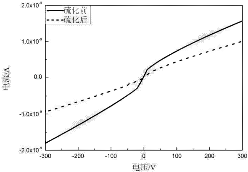
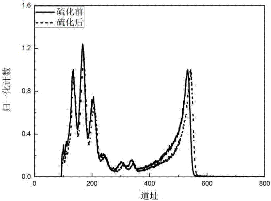
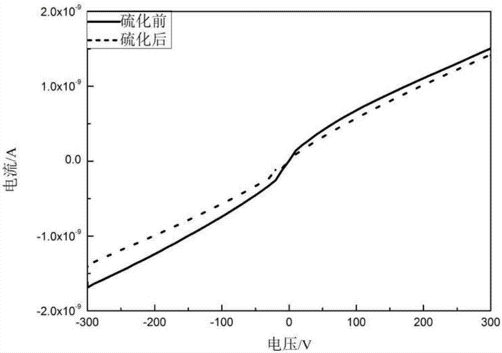
The invention discloses a CdZnTe planar detector surface treatment method and is to solve the technical problem of poor energy resolution of a planar detector obtained after processing of an existing planar detector surface treatment method. The technical scheme is characterized by, after corrosion of a CdZnTe wafer, carrying out passivation on the surface of the CdZnTe wafer through a (NH4)2S solution; carrying out cleaning after passivation through deionized water; and finally, plating an Au electrode onto the two surfaces of the wafer through a vacuum evaporator. Through the passivation method, a Te-rich layer is removed, a CdS layer is deposited on the surface of the wafer, and stoichiometric ratio is improved, thereby reducing scattering of electrons on the surface of the crystal; dangling bonds formed after corrosion are neutralized, thereby reducing leak current on the surface of the CdZnTe wafer, improving energy resolution and improving detection efficiency of the CdZnTe planar detector; and through test, the energy resolution of the CZT planar detector is improved from original energy resolution larger than 6.5% to energy resolution smaller than 4.5%.

Description

technical field [0001] The invention relates to a method for treating the surface of a plane detector, in particular to a method for treating the surface of a CdZnTe plane detector. Background technique [0002] CdZnTe is by far the most ideal semiconductor material for manufacturing room temperature γ-ray and X-ray detectors and infrared thin film epitaxial substrates such as HgCdTe. This ideal room temperature nuclear radiation semiconductor material has attracted attention in many fields and is suitable for X-ray fluorescence analysis. , Astrophysics, safety inspection, environmental protection, ecology, nuclear medicine and clinical medicine and other fields, it has become an upgraded product replacing traditional detectors and scintillator detectors. The surface quality of its wafer is a key factor affecting the performance of the detector. [0003] CdZnTe wafers can be tested for performance after four steps of mechanical polishing, chemical corrosion, surface passiva...

Claims


Application Information

Patent Timeline
Patent Type & Authority Applications(China)
IPC IPC(8): H01L31/08H01L31/18
CPCH01L31/085H01L31/1868Y02P70/50
Inventor 介万奇侯文欣王涛查钢强徐凌燕
Owner NORTHWESTERN POLYTECHNICAL UNIV
Learn More