Schottky gate field effect transistor and preparation method and application thereof

A technology of field effect transistor and Schottky gate, which is applied in the field of microelectronics, can solve the problems that the research on Schottky gate electrode has not been reported, and can not solve the problem of short channel effect well, so as to improve the switching performance and size Small, the effect of suppressing leakage current

Inactive Publication Date: 2017-09-08
GUANGDONG UNIV OF TECH
View PDF4 Cites 8 Cited by
  • Summary
  • Abstract
  • Description
  • Claims
  • Application Information

AI Technical Summary

Problems solved by technology

However, the current two-dimensional material Schottky device is mainly the Schottky contact of the source and drain electrodes, which cannot solve the problem of short channel effect well, and the research on the Schottky gate electrode has not been reported yet.

Method used


Image

  • Schottky gate field effect transistor and preparation method and application thereof
  • Schottky gate field effect transistor and preparation method and application thereof

Examples


Embodiment 1

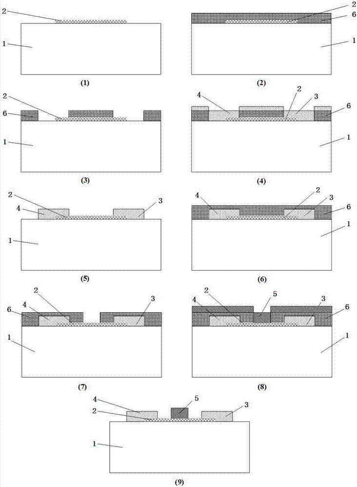
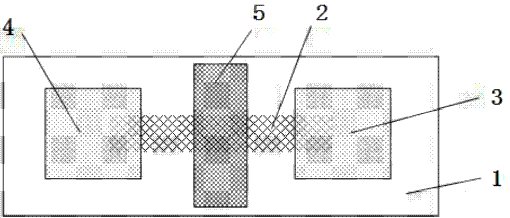
[0030] figure 1 It is a schematic flow chart of the preparation method of a Schottky gate field effect transistor, wherein 1 is a substrate, 2 is a two-dimensional material, 3 is a source electrode, 4 is a drain electrode, 5 is a Schottky gate electrode, 6 is a photoresist, Include the following steps:

[0031] 1. Utilize the method of chemical vapor deposition to prepare WS on the silicon wafer substrate 1 2 2D Materials 2, WS 2 The thickness is 0.5nm, such as figure 1 (1) shown.

[0032] 2. On the silicon wafer substrate 1 and WS 2 A photoresist 6 with a thickness of 2 μm is spin-coated on the two-dimensional material 2, such as figure 1 (2) shown.

[0033] 3. Photolithography exposure and development ( figure 1 (3) shown), after carrying WS 2 The silicon wafer substrate 1 sample of the two-dimensional material 2 is plated with Ti with a thickness of 50 nm to form a source electrode 3 and a drain electrode 4, such as figure 1 (4) shown.

[0034] 4. Wash off the pho...

Embodiment 2

[0040] The difference from Example 1 is that the two-dimensional material is ZrSe 2 , ZrSe 2 The thickness is 20nm; the annealing temperature is 500°C, the gas atmosphere is Ar; the Schottky gate electrode is metal Ni, and the thickness of Ni is 1000nm.


PUM


Abstract

The invention discloses a preparation method of a schottky gate field effect transistor. According to the preparation method, a two-dimensional material is prepared on a substrate firstly, then the substrate and the two-dimensional material are coated with photoresist in a spin coating manner, and photoetching exposure and developing are performed to expose source and drain electrode windows; metal is coated, and the photoresist is washed off, and next, annealing in gas atmosphere is performed to form a source electrode and a drain electrode; next, the whole piece of a sample is coated with photoresist in a spin coating manner, and photoetching exposure and developing are performed to expose a gate electrode window; and next, metal is coated, and the photoresist is washed off to form the schottky gate field effect transistor. The schottky gate field effect transistor has the advantages of small dimensions, high switch ratio, high mobility, capability of well eliminating a short-channel effect and the like, so that the application field of a two-dimensional material device can be expanded.

Description

technical field [0001] The invention belongs to the technical field of microelectronics, and more specifically relates to a Schottky gate field effect transistor and its preparation method and application. Background technique [0002] As the earliest discovered two-dimensional material, graphene has attracted a lot of attention and research in recent years due to its unique physical and chemical properties and great application potential in the field of nano-optoelectronics. However, the zero-bandgap property of graphene limits its application in the field of nanoelectronics. Although people use various methods to open its band gap, the opened band gap is very small and has little effect. In recent years, as an alternative to graphene, two-dimensional transition metal chalcogenides (TMDs) are gradually emerging, they have a certain size band gap (1-3eV) and exhibit excellent optoelectronic properties. For example, based on single-layer or few-layer MoS 2 The field effect...

Claims


Application Information

Patent Timeline
Patent Type & Authority Applications(China)
IPC IPC(8): H01L29/78H01L29/423H01L21/336
Inventor 杨炎锋杨亿斌招瑜肖也罗东向牟中飞李京波
Owner GUANGDONG UNIV OF TECH
Why Eureka
Try Eureka