Visible infrared broad band absorber and preparation method thereof

An absorber and broadband technology, applied in the field of visible to infrared broadband absorber and its preparation, can solve the problems of low efficiency, high cost, complicated preparation process, etc.

Inactive Publication Date: 2017-09-19
SHANGHAI INST OF TECHNICAL PHYSICS - CHINESE ACAD OF SCI
View PDF4 Cites 6 Cited by
  • Summary
  • Abstract
  • Description
  • Claims
  • Application Information

AI Technical Summary

Problems solved by technology

These methods can indeed broaden the working wavelength of the system, but the preparation of materials usually requires advanced modern micro-nano proc

Method used


Image

  • Visible infrared broad band absorber and preparation method thereof
  • Visible infrared broad band absorber and preparation method thereof
  • Visible infrared broad band absorber and preparation method thereof

Examples


Embodiment 1

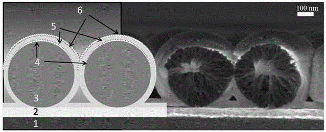
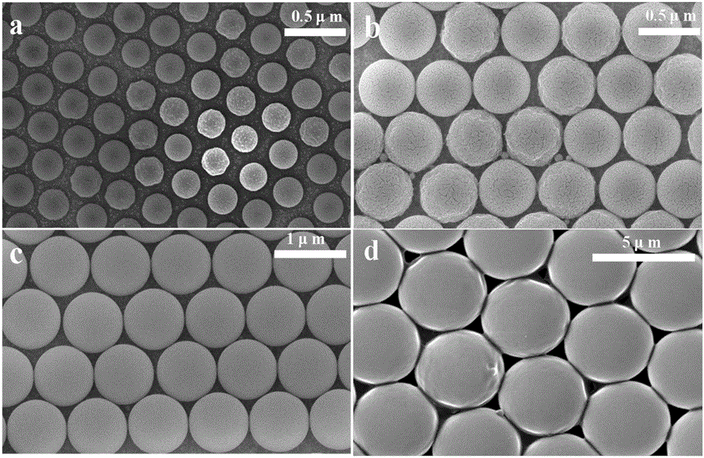
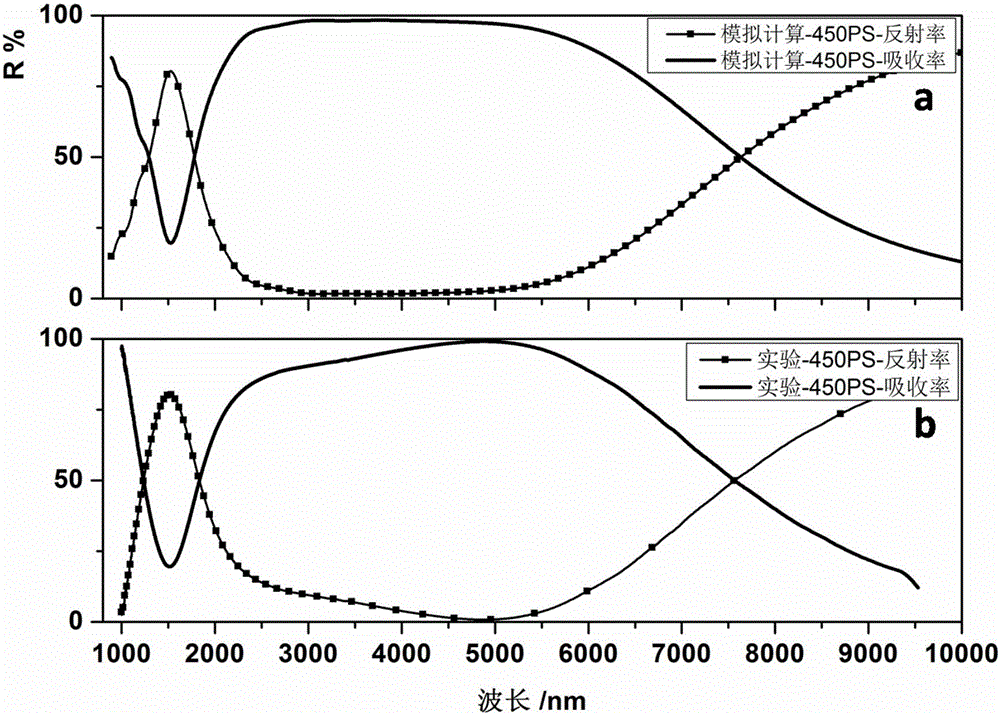
[0020] A 100nm gold (Au) thin film was deposited on a silicon substrate by thermal evaporation, and a monolayer of PS balls was formed on the film by self-assembly of polystyrene (PS) balls. The PS spheres we use are 10 wt% aqueous solutions of polystyrene spheres produced by Thermo Scientific. The diameter of PS pellets is 400 nm. Then a 5nm gold film is deposited by thermal evaporation, a 10nm zinc oxide film is deposited by metal organic chemical vapor phase, and a 5nm gold film is deposited on the outermost layer by thermal evaporation. The sample is tested, and the obtained absorption spectrum is greater than 90% at 1.5-2.4 μm, the peak absorption rate (98%), and the full width at half maximum is (0.5 μm).

Embodiment 2

[0022] A 100nm gold thin film is electron beam evaporated on a glass substrate, and a monolayer of PS spheres is formed on the film by self-assembly of polystyrene (PS) spheres. The PS spheres used are 10 wt% aqueous solutions of polystyrene spheres produced by Thermo Scientific. The diameter of PS pellets is 400 nm. Then a 5nm gold film is evaporated by electron beam, a 30nm aluminum oxide film is deposited by atomic layer, and a 5nm gold film is sputtered on the outermost layer by an argon ion beam. The sample is tested, and the obtained absorption spectrum is greater than 90% at 1.5-2.9 μm, the peak absorption rate (95%), and the full width at half maximum is (0.7 μm).

Embodiment 3

[0024] A 100nm gold film was sputtered by argon ion beams on a GaAs substrate, and a monolayer of PS balls was formed on the film by self-assembly of polystyrene (PS) balls. The PS spheres we use are 10 wt% aqueous solutions of polystyrene spheres produced by Thermo Scientific. The diameter of the PS ball is 500nm, which is etched to 300nm by oxygen ion, then a 5nm gold film is sputtered by an argon ion beam, a 100 nm zinc oxide film is magnetron sputtered, and a 5nm gold film is sputtered on the outermost layer by an argon ion beam gold film. The sample is tested, and the obtained absorption spectrum is greater than 85% at 2-3.8 μm, the peak absorption rate (98%), and the full width at half maximum is (0.9 μm).


PUM

PropertyMeasurementUnit
Diameteraaaaaaaaaa
Thicknessaaaaaaaaaa
Thicknessaaaaaaaaaa

Abstract

The present invention discloses a visible infrared broad band absorber and a preparation method thereof. The device is formed by a multilayer structure consisting of a metal bottom layer, a polymer granular layer, a metal interface layer, a dielectric layer and a metal outer layer in order from a substrate to up. The operating wavelength of the absorber can cover the visible light wave band ( 0.4-0.8[Mu]m) and shortwave infrared band ( 1.1-3[Mu]m), medium wave infrared band ( 3-6[Mu]m) and long wave infrared band ( 6-14[Mu]m). The peak value absorptivity A can reach 99%, and the full width at half-maximum can reach 2[Mu]m. The visible infrared broad band absorber is high in absorption efficiency, wide in operation band and adjustable in wavelength; the visible infrared broad band absorber is not sensitive to incident light polarization and angle; and the visible infrared broad band absorber is simple in technology and low in cost, can perform large-scale preparation and can be grown on a flexible substrate, etc.

Description

technical field [0001] The invention relates to the technical field of optical devices, and relates to a visible to infrared broadband absorber and a preparation method thereof. Background technique [0002] Broadband perfect absorbers have always been a hot topic in the field of science and technology, especially broadband absorption in the visible and infrared bands, because of their important application requirements in many fields such as solar energy harvesting, infrared detection, information sensing, and photothermal utilization. extensive attention. Traditional enhanced absorption methods usually use the absorption properties of the material itself combined with anti-reflection and anti-reflection means, or use a more complex structural system to achieve the purpose of broadband absorption. These methods have their own characteristics, but the general system is relatively thick or can only work in a specific band. [0003] The emergence of plasmonic metamaterials p...

Claims


Application Information

Patent Timeline
IPC IPC(8): G02B5/00
CPCG02B5/003
Inventor 俞伟伟孙艳陈鑫郝加明王书霞戴宁
Owner SHANGHAI INST OF TECHNICAL PHYSICS - CHINESE ACAD OF SCI
Why Eureka
Try Eureka