GaNHEMT cell structure with graphene buried source and longitudinal gate and preparation method

A graphene and source technology, applied in electrical components, semiconductor/solid-state device manufacturing, circuits, etc., can solve the problems of hidden reliability, small device threshold voltage, poor uniformity, etc., and achieve stable high threshold voltage and low Effects of on-resistance, reduced gate on-resistance, good repeatability and uniformity

Pending Publication Date: 2017-09-22
BEIJING HUAJINCHUANGWEI ELECTRONICS CO LTD
View PDF10 Cites 4 Cited by
  • Summary
  • Abstract
  • Description
  • Claims
  • Application Information

AI Technical Summary

Problems solved by technology

The fluorine ion implantation barrier layer scheme does not damage the 2DEG channel interface, but due to the thermal stability of fluorine ions, the reliability of the device during use is a potential hidden danger. In addition, for large-area devices, the threshold voltage uniformity is not good
[0006] like image 3 As shown, the normally-off device structure with a p-type GaN (or InGaN) capping layer grown above the gate barrier layer uses the built-in electric field to deplete the 2DEG channel electrons, and the device channel conducts better, but the high concentration p Type doping is difficult to control, and the concentration uniformity of each position of the epitaxial wafer is not completely consistent, so the threshold voltage of the device is small and the uniformity is also not good
In addition, because the gate electrode is too far away from the 2DEG channel, the switching rate of the device is affected

Method used


Image

  • GaNHEMT cell structure with graphene buried source and longitudinal gate and preparation method
  • GaNHEMT cell structure with graphene buried source and longitudinal gate and preparation method
  • GaNHEMT cell structure with graphene buried source and longitudinal gate and preparation method

Examples


Embodiment Construction

[0029] The present invention will be described more fully below using examples. This invention may be embodied in many different forms and should not be construed as limited to the exemplary embodiments set forth herein.

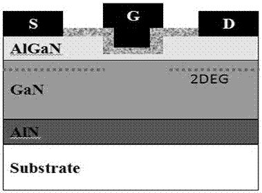
[0030] like Figure 4 As shown, the GaN HEMT device in this embodiment adopts the GaN HEMT cell structure of the graphene buried source and the vertical gate, including the substrate, the AlN layer and the graphene buried heat dissipation layer, the AlN isolation layer, the GaN buffer layer, channel layer and AlGaN barrier layer. A through hole to the graphene layer is etched next to the source, and the graphene buried heat dissipation layer is connected to the source of the device through the metal passing through the above through hole, which plays the role of source grounding, and utilizes the high thermal conductivity of graphene to connect the The heat generated in the channel area of ​​the device is quickly conducted away, making the temperature rise...


PUM


Abstract

The invention discloses a GaNHEMT cell structure with a graphene buried source and a longitudinal gate. The source is connected with a graphene buried cooling layer through a metal material; the device adopts a longitudinal gate structure, a long transverse channel opening mode in the traditional HEMT device is turned to a short longitudinal channel opening mode, a long transverse current control channel is turned to a short longitudinal current control channel for the gate, the device uses a short gate side wall channel to realize switch control, and the on resistance of the device can be effectively reduced. A high-density cell structure can be realized, and the effective using area and the unit area power density of the device are improved; and by using the excellent thermal conductivity of the graphene, heat generated in an active area of the device can be conducted rapidly, the high-power GaNHEMT device can be realized, and the high-temperature reliability of the device can be enhanced.

Description

technical field [0001] The invention relates to a novel GaN HEMT cell structure with a graphene buried source and a vertical grid, belonging to the technical field of semiconductor devices. Background technique [0002] As the core components of power converters such as DC / AC, AC / DC, DC / DC, and AC / AC, power switching devices have important application requirements in modern electronic equipment. They are important for realizing integrated control of related systems and ensuring system safety and reliability. The key core device for performance, stability and efficiency. GaN is a typical representative of the third-generation wide bandgap semiconductor material. Compared with the traditional semiconductor material Si, GaN has a wide bandgap, a large breakdown electric field, a high electron saturation drift velocity, a small dielectric constant, and good chemical stability. Features. GaN material heterostructure (typically such as AlGaN / GaN) interface has a large density of...

Claims


Application Information

Patent Timeline
Patent Type & Authority Applications(China)
IPC IPC(8): H01L29/423H01L21/336H01L29/778
CPCH01L29/4232H01L29/66431H01L29/778
Inventor 袁俊李百泉倪炜江张敬伟牛喜平李明山耿伟徐妙玲
Owner BEIJING HUAJINCHUANGWEI ELECTRONICS CO LTD
Why Eureka
Try Eureka