A silicon carbide trenchmos device and manufacturing method thereof
A technology of silicon carbide and devices, applied in semiconductor/solid-state device manufacturing, semiconductor devices, electric solid-state devices, etc., can solve problems such as high power loss, high production cost, and low work efficiency
- Summary
- Abstract
- Description
- Claims
- Application Information
AI Technical Summary
Problems solved by technology
Method used
Image
Examples
Embodiment 1
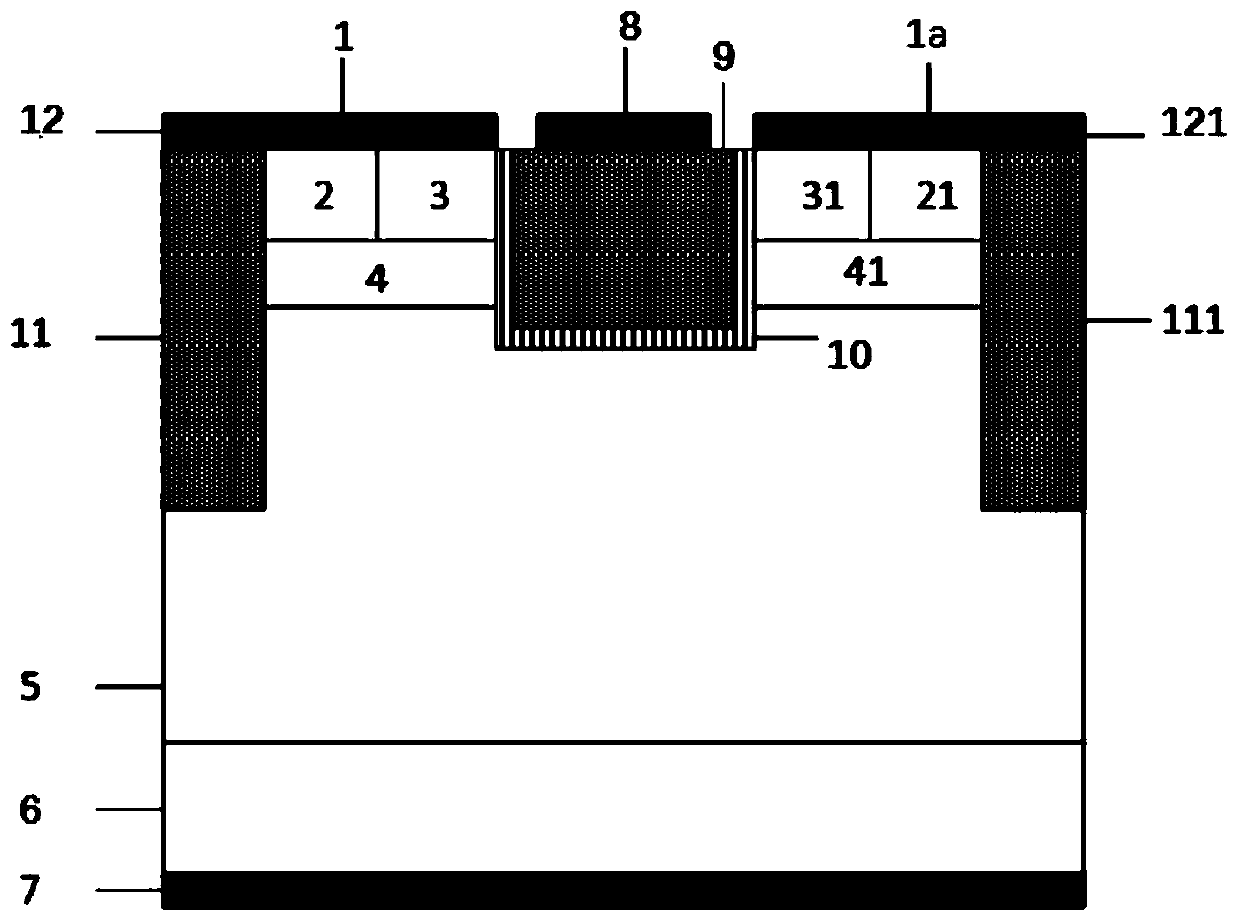
[0099] A silicon carbide Trench MOS device, its cell structure is as follows figure 2 Shown includes: metal drain electrodes 7, N + Substrate 6 and N - Epitaxial layer 5; characterized in that: the N - The two ends of the upper layer of the epitaxial layer 5 respectively have first P + polysilicon region 11 and the second P + polysilicon region 111, the first P + polysilicon region 11 and the second P + The upper surface of the polysilicon region 111 is respectively provided with a first metal electrode 12 and a second metal electrode 121; + N between the polysilicon regions 11, 111 - The epitaxial layer 5 has a Trench gate structure, and the Trench gate structure includes a polysilicon gate 9, a gate oxide layer 10 disposed on the bottom surface and sidewalls of the polysilicon gate 9, and a metal gate 8 disposed on the upper surface of the polysilicon gate 9; + N between the polysilicon region 11 and the Trench gate structure - The upper layer of the epitaxial layer ...
Embodiment 2
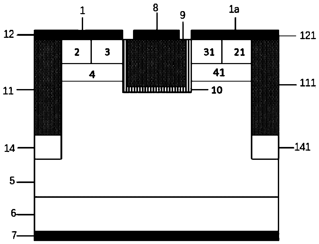
[0102] This implementation except in the first P + polysilicon region 11 and the second P + There is a first P in contact with the polysilicon region 111 below + SiC region 14 and the second P + SiC region 141; the P +The width of the silicon carbide region 14, 141 and P + The polysilicon region 11 has the same width, as image 3 shown.
[0103] The P added in this embodiment + The SiC region 14, 141 is able to P + The polysilicon regions 11, 111 and the trench gate play the role of electric field shielding, thereby improving the withstand voltage of the device, and have a certain effect on suppressing the reverse leakage current.
Embodiment 3
[0105] This implementation except in the first P + polysilicon region 11 and the second P + There is a first P in contact with the polysilicon region 111 below + SiC region 14 and the second P + SiC region 141; the P + The width of the silicon carbide region 14, 141 is greater than P + The width of the polysilicon region 11, such as Figure 4 As shown, in this implementation P + The width of the silicon carbide regions 14 and 141 ranges from 1.0 to 2.6 μm.
[0106] In this example, P + The silicon carbide regions 14, 141 have larger lateral dimensions (i.e., widths), which have a stronger electric field shielding effect on the P+ polysilicon regions 11, 111 and trench gates compared to Example 2, further improving the withstand voltage of the device, and at the same time The reverse leakage current is also further suppressed.
PUM
| Property | Measurement | Unit |
|---|---|---|
| thickness | aaaaa | aaaaa |
| thickness | aaaaa | aaaaa |
| thickness | aaaaa | aaaaa |
Abstract
Description
Claims
Application Information


