QLED, preparation method and display apparatus

A dendritic, light-emitting layer technology, applied in semiconductor/solid-state device manufacturing, electrical components, circuits, etc., can solve problems affecting QLED light-emitting performance

Active Publication Date: 2017-11-17
HISENSE VISUAL TECH CO LTD
View PDF11 Cites 27 Cited by
  • Summary
  • Abstract
  • Description
  • Claims
  • Application Information

AI Technical Summary

Problems solved by technology

[0005] The application provides a QLED, a preparation method and a display device to solve the technical problem that the long-chain ligands of quantum dots affect the luminous performance of QLED

Method used


Image

  • QLED, preparation method and display apparatus
  • QLED, preparation method and display apparatus
  • QLED, preparation method and display apparatus

Examples


Embodiment 1

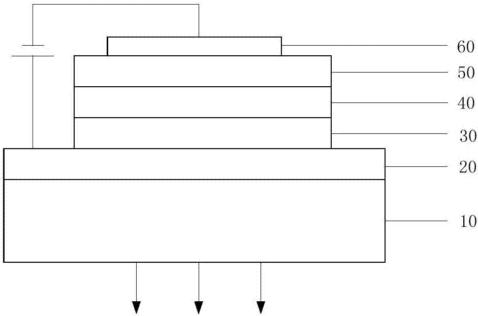
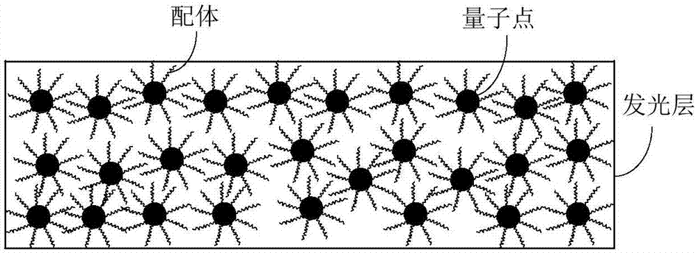
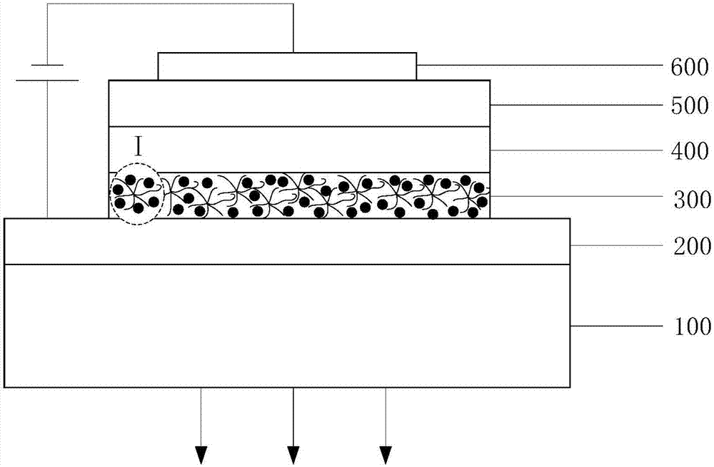
[0021] Embodiment 1 of the present application aims at the problem that the long-chain ligands on the surface of quantum dots in the existing QLED light-emitting layer will affect the light-emitting performance of the QLED, and provides a QLED. image 3 and Figure 4 are respectively a structural schematic diagram of a QLED provided in Embodiment 1 of the present application and image 3 Partial enlarged view of center I. Depend on image 3 and Figure 4 It can be seen that the QLED sequentially includes a substrate 100, an anode 200, a hole transport layer 300, a light emitting layer 400, an electron transport layer 500, and a cathode 600, wherein the light emitting layer 300 includes quantum dots and a dispersant having a dendritic molecular structure, The quantum dots are dispersed between the side chains of the dendrimers.

[0022] In this embodiment, a dispersant having a dendritic molecular structure is used to disperse the quantum dot material, so that the quantum d...

Embodiment 2

[0027] Embodiment 2 of the present application provides a method for preparing the QLED described in Embodiment 1. Figure 5 It is a method flowchart of a method for preparing a QLED provided in Example 2 of the present application. Depend on Figure 5 It can be seen that the method includes:

[0028] Step S201: Spin-coat a hole transport layer, a light emitting layer, and an electron transport layer sequentially on the patterned ITO substrate to form a mixed layer sample, wherein the light emitting layer includes quantum dots and a dispersant with a dendritic molecular structure, so The quantum dots are dispersed between the side chains of the dendrimers.

[0029] Step S202: Evaporating a cathode on the surface of the mixed layer sample.

[0030] In the step S201 of this embodiment, before the hole transport layer is spin-coated, a step of spin-coating the hole injection layer may also be included.

Embodiment 3

[0032] This embodiment provides a method for preparing a QLED, the method comprising:

[0033] Step S301: preparing CdSe / ZnSeS / ZnS quantum dots by hydrothermal method.

[0034]The CdSe / ZnSeS / ZnS quantum dots prepared in this example have a three-layer core-shell structure, the inner core is ZnCdSe, the outer shell is ZnS, and the CdSe / ZnSeS / ZnS quantum dots have strong optical stability. The preparation method is as follows: mix cadmium oxide and amine oxide with a molar ratio of 1:4 in an argon atmosphere, heat to 100°C and keep it warm for 30 minutes, then heat to 220°C to obtain cadmium oleate, and cool the cadmium oleate to room temperature for later use; under anaerobic conditions, dissolve selenium in 5 times the mass of tributyl phosphate, and then add 5 times the mass of octadecene ODE to prepare the selenium solution for later use; quickly add the selenium solution to the cadmium oleate , heated to 260°C and held for 40min. By controlling the holding time (that is, ...


PUM


Abstract

The invention provides a QLED, a preparation method and a display apparatus. The QLED comprises a substrate, a positive electrode, a hole transport layer, a light emitting layer, an electron transport layer and a negative electrode in sequence; the light emitting layer comprises quantum dots and a dispersing agent with a dendritic molecular structure; and the quantum dots are dispersed among side chains of the dendritic molecules. Compared with long-chain ligands on the surfaces of the quantum dots, an insulating layer is not formed on the surfaces of the quantum dots in the dendritic molecular structure, so that charge injection potential barrier of impedance, holes and electrons to the quantum dots on the surfaces of the quantum dots can be greatly lowered; in addition, the spacings between the quantum dot molecules, between quantum dots and the electron transport layer, and between the quantum dots and the hole transport layer can be closer, thereby improving the concentration of the quantum dots in the light emitting layer, and the exciton energy transfer efficiency; and by virtue of the OLED, the dispersity and yield of the quantum dots can be ensured while the current carrier energy transfer validity can be reinforced, thereby enhancing the light emitting efficiency of the OLED and the luminance of the OLED display apparatus.

Description

technical field [0001] The present application relates to the field of display technology, in particular to a QLED, a manufacturing method and a display device. Background technique [0002] With the continuous development of the TV industry, high color gamut displays have become the mainstream trend of the TV industry. ) technology-based QLED display, in addition to the advantages of a wide color gamut, it also has many advantages such as high brightness, fast response speed, and better HDR effects, and has a very broad application prospect. [0003] figure 1 It is a schematic structural diagram of a common QLED. Such as figure 1 As shown, the flexible QLED display screen includes a substrate 10 , an anode layer 20 , a hole transport layer 30 , a light emitting layer 40 , an electron transport layer 50 and a cathode layer 60 in sequence. When an appropriate voltage is applied between the anode layer 20 and the cathode layer 60 of the QLED display, the holes in the anode...

Claims


Application Information

Patent Timeline
Patent Type & Authority Applications(China)
IPC IPC(8): H01L51/50H01L51/56H01L51/54
CPCH10K85/111H10K50/115H10K71/00
Inventor 刘振国宋志成刘卫东
Owner HISENSE VISUAL TECH CO LTD
Why Eureka
Try Eureka