A pretreatment method for growing single crystal orientation zinc oxide

A zinc oxide and pretreatment technology, applied in the semiconductor field, can solve the problems of limited application, poor crystallization quality of zinc oxide film, etc., and achieve good preparation effect

Active Publication Date: 2019-10-29
INST OF MICROELECTRONICS CHINESE ACAD OF SCI
View PDF9 Cites 0 Cited by
  • Summary
  • Abstract
  • Description
  • Claims
  • Application Information

AI Technical Summary

Problems solved by technology

Among them, chemical vapor deposition technology (CVD) and atomic layer deposition technology (ALD) often present polycrystalline films due to the poor crystallization quality of the prepared zinc oxide films, which greatly limits their application in the semiconductor industry.

Method used


Image

  • A pretreatment method for growing single crystal orientation zinc oxide
  • A pretreatment method for growing single crystal orientation zinc oxide
  • A pretreatment method for growing single crystal orientation zinc oxide

Examples


Embodiment 1

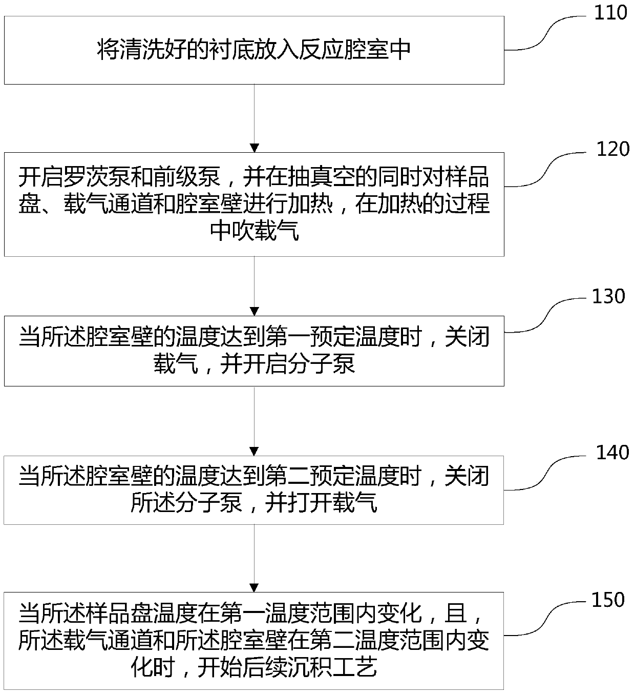
[0030] Such as figure 1 As stated, the embodiment of the present invention provides a pretreatment method for growing zinc oxide with a single crystal orientation, the method comprising:

[0031] Step 110: Put the cleaned substrate into the reaction chamber;

[0032] Specifically, cleaning the substrate adopts a sapphire cleaning step to clean the substrate, and the specific process also includes:

[0033] Step 101: put the substrate in acetone and ultrasonically perform the first predetermined time, and blow it dry after taking it out;

[0034] Step 102: Put the substrate into the isopropanol solution and sonicate for a second predetermined time, and blow it dry after taking it out;

[0035] Step 103: put the substrate in deionized water and ultrasonically for a third predetermined time, and blow it dry after taking it out.

[0036] The first predetermined time, the second predetermined time and the third predetermined time are dynamically adjusted by those skilled in the ...

Embodiment approach

[0054] In order to more clearly illustrate the technical solutions and technical effects of the embodiments of the present invention, the present invention provides specific implementation solutions, the specific contents of which are as follows:

[0055] Put the sapphire substrate with C-axis single orientation into acetone, isopropanol and deionized water and ultrasonically clean it for 5 minutes, take it out and dry it, and put it into the chamber of the atomic layer deposition equipment. Turn on the foreline pump and Roots pump of the equipment, heat the sample tray, chamber wall and carrier gas channel at the same time, and set the heating temperature to 200°C, 100°C and 110°C respectively, and feed high-purity nitrogen as carrier gas during the heating process. When the chamber wall temperature rises to 80°C, the molecular pump is turned on, the carrier gas is turned off, and the molecular pump is stopped until the chamber wall temperature rises to 100°C. After the molec...


PUM


Abstract

The invention discloses a pretreatment method for growing one-crystal orientation zinc oxide, and belongs to the technical field of semiconductors. According to the embodiment of the invention, the pretreatment method adopts the technical steps of putting a cleaned substrate into a reaction chamber; powering on a roots pump and a backing pump, heating a sample disc, a gas carrying channel and a chamber wall while vacuuming, and blowing a carrying gas in the heating process; when the temperature of the chamber wall reaches first preset temperature, cutting off the carrying gas, and powering on a molecular pump; when the temperature of the chamber wall reaches second preset temperature, powering off the molecular pump, and opening the carrying gas; and when the temperature of sample disc is changed within a first temperature range, and the gas carrying channel and the chamber wall are changed within a second temperature range, starting a later deposition process, and thus a technical effect of relatively well preparing a single crystal zinc oxide membrane is achieved.

Description

technical field [0001] The invention relates to the technical field of semiconductors, in particular to a pretreatment method for growing zinc oxide with a single crystal orientation. Background technique [0002] With the continuous development of semiconductor technology, semiconductor thin films play a very important role in high-tech industries such as microelectronics, optics, and informatics. The preparation and doping technology of high crystal quality semiconductor thin films is developed, especially for the third generation semiconductor The preparation, characterization, doping and characteristics research of the material ZnO thin film are of great significance to important application fields for new energy, including ultraviolet light-emitting materials, ultraviolet detectors, highly integrated photonics and electronic devices, solar cells, etc. . [0003] Zinc oxide, as a new type II-VI group direct bandgap wide bandgap compound, has a large room temperature ban...

Claims


Application Information

Patent Timeline
Patent Type & Authority Patents(China)
IPC IPC(8): C30B25/00C30B29/16
CPCC30B25/00C30B29/16
Inventor 张思敏夏洋卢维尔程嵩李楠
Owner INST OF MICROELECTRONICS CHINESE ACAD OF SCI
Why Eureka
Try Eureka