Polycrystalline silicon wafer back polishing technology

A backside polishing, polycrystalline silicon wafer technology, applied in sustainable manufacturing/processing, electrical components, climate sustainability, etc., can solve the problems of increased reflection, low absorption, rough etching on the back of the battery, etc., to improve short-circuit current and, The effect of reducing the probability of damage and improving the light absorption efficiency

Inactive Publication Date: 2017-12-19
TONGWEI SOLAR (ANHUI) CO LTD
View PDF8 Cites 1 Cited by
  • Summary
  • Abstract
  • Description
  • Claims
  • Application Information

AI Technical Summary

Problems solved by technology

[0003] The conversion efficiency of solar cells is an important standard to measure the technical level of a photovoltaic enterprise. The traditional battery production line can no longer greatly improve the efficiency. However, although the new selective emitter cells and N-type cells have improved the efficiency, they have also greatly increased Reduced equipment costs and process risks, the back of traditional batteries is etched rough, resulting in low light absorption in the silicon wafer, affecting short-circuit current
In order to solve the above-mentioned problems of rough etching and low light absorption rate on the back of the battery, a new back polishing process for silicon wafers was proposed in the publication No. "201210456821. The use of the battery can significantly improve the conversion efficiency of the battery, and it can increase the reflection of light inside the battery, effectively improve the absorption of long-wave light, and effectively increase the short-circuit current of the battery. In addition, this process can be directly realized on the traditional production line without new Additional equipment
[0004] However, for the above-mentioned process of "a method for preparing a back-polished silicon wafer", we have found in practice that there are some problems that can be improved in the process steps to achieve process optimization. The problems are mainly reflected in: 1. Silicon in the above process After the etching is completed, the silicon wafer is soaked in hydrofluoric acid, because after the etching is completed, a phosphosilicate glass layer will be formed on the diffusion surface of the silicon wafer, and the acid solution will corrode the phosphosilicate glass layer, and further damage the diffusion surface of the silicon wafer. Cause damage and affect the suede surface of the diffusion surface; 2. When using lye to polish silicon wafers, the soaking time is longer. Long-term soaking not only reduces polishing efficiency, but also causes damage to silicon wafers; 3. Using acid After neutralizing the lye for polishing, the ions generated after neutralization will remain on the silicon wafer. When using pure water to rinse, the above-mentioned process time is short, and the residue cannot be rinsed well. For subsequent silicon wafers The preparation process affects

Method used


Image

  • Polycrystalline silicon wafer back polishing technology

Examples


Embodiment 1

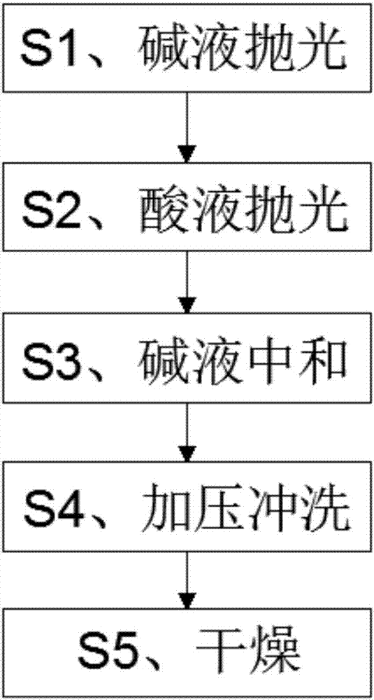
[0027] A process for polishing the back of a polysilicon wafer, comprising the following steps:

[0028] Step S1, lye polishing: In order to only soak the back of the silicon wafer, use a commonly used chain etching machine, add strong lye to the chain etcher, adjust the height of the strong lye in the machine tank, use the viscous roller to only The back of the silicon wafer is soaked, and the strong alkali solution is a mixed solution of sodium hydroxide and potassium hydroxide, wherein the mass concentration of the sodium hydroxide solution is 15%, and the mass concentration of the potassium hydroxide solution is 10%, and the sodium hydroxide and potassium hydroxide The volume ratio of potassium is 1:0.75, soak the back of the silicon wafer for 10s, and control the soaking temperature to 10°C throughout the process.

[0029] Step S2, acid polishing: take out the silicon wafer after soaking in step S1, and then use the chain etching machine of the same model as step S1, add ...

Embodiment 2

[0035] A process for polishing the back of a polysilicon wafer, comprising the following steps:

[0036] Step S1, lye polishing: In order to only soak the back of the silicon wafer, use a commonly used chain etching machine, add strong lye to the chain etcher, adjust the height of the strong lye in the machine tank, use the viscous roller to only The back of the silicon wafer is soaked, and the strong alkali solution is a mixed solution of sodium hydroxide and potassium hydroxide, wherein the mass concentration of the sodium hydroxide solution is 15%, and the mass concentration of the potassium hydroxide solution is 10%, and the sodium hydroxide and potassium hydroxide The volume ratio of potassium is 1:0.75, soak the back of the silicon wafer for 20s, and control the soaking temperature to 5°C throughout the process.

[0037] Step S2, acid polishing: take out the silicon wafer after soaking in step S1, and then use the chain etching machine of the same model as step S1, add w...


PUM


Abstract

The invention discloses a polycrystalline silicon wafer back polishing technology. The polycrystalline silicon wafer back polishing technology comprises the following steps: step S1, alkali liquor polishing: soaking the back of a silicon wafer with a strong alkali liquor; step S2, acid liquor polishing: taking out the silicon wafer after soaking in step S1, and soaking the back of the silicon wafer with a weak acid liquor; step S3, alkali liquor neutralization: taking out the silicon wafer after soaking in step S2, and washing the back of the silicon wafer with a weak alkali liquor; step S4, taking out the silicon wafer in step S3, and washing the back of the silicon wafer with pure water through a pressurization gun; and step S5, drying: drying the silicon wafer obtained in step S4 by using an air knife. Under the conditions that the time used in the polishing technology is shorter, the damage on the silicon wafer is lower and the washing effect of the silicon wafer is better, the back polishing effect of the silicon wafer can be effectively strengthened, the back light absorption efficiency of the silicon wafer is promoted, and then the short-circuit current of the silicon wafer and the conversion efficiency of the silicon wafer are effectively improved.

Description

technical field [0001] The invention relates to the technical field of silicon wafer preparation technology, in particular to a polycrystalline silicon wafer back polishing process. Background technique [0002] In the past ten years, solar photovoltaic power generation has become one of the fastest-growing branches of new energy. Crystalline silicon solar cells are the most widely used cell type in solar photovoltaic power generation. [0003] The conversion efficiency of solar cells is an important standard to measure the technical level of a photovoltaic enterprise. The traditional battery production line can no longer greatly improve the efficiency. However, although the new selective emitter cells and N-type cells have improved the efficiency, they have also greatly increased The equipment cost and process risk are reduced, and the backside of the traditional battery is etched rough, resulting in low light absorption in the silicon wafer, which affects the short-circui...

Claims


Application Information

Patent Timeline
Patent Type & Authority Applications(China)
IPC IPC(8): H01L21/306H01L21/304H01L31/18
CPCH01L21/304H01L21/306H01L31/1876Y02P70/50
Inventor 苏世杰李强强张玉前郭俊张欢
Owner TONGWEI SOLAR (ANHUI) CO LTD
Why Eureka
Try Eureka