
Back polishing process of solar cell sheet

A technology for back polishing of solar cells, applied in circuits, photovoltaic power generation, electrical components, etc., can solve the problems of no light, short process time, long soaking time, etc., to reduce the probability of damage and improve the quality of polishing , the effect of saving time

Active Publication Date: 2019-05-31
中建材浚鑫(桐城)科技有限公司
View PDF7 Cites 2 Cited by
  • Summary
  • Abstract
  • Description
  • Claims
  • Application Information

AI Technical Summary

Problems solved by technology

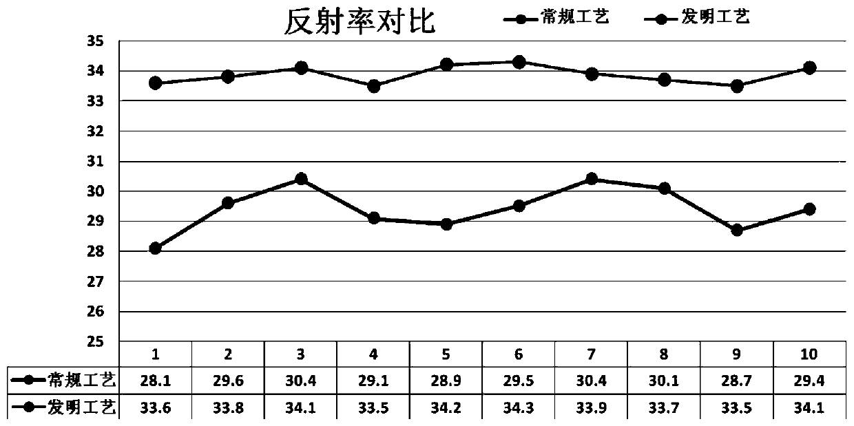
[0003] Although the current solar cell back polishing process has the above-mentioned advantages, there are also the following disadvantages: when using lye to polish silicon wafers, the immersion time is long, and long-term immersion not only reduces the polishing efficiency, but also damages the silicon wafers. Cause damage; after using acid to neutralize the polishing lye, the ions generated after neutralization will remain on the silicon wafer. When using pure water to rinse, the above process time is short, and the residue cannot be fully rinsed , which will affect the subsequent silicon wafer preparation process; although the current solar cell back polishing process can play a certain role in back polishing, the polishing effect is not good. The light in the wavelength band (wavelength greater than 1000nm) is absorbed; there is only KOH in the alkali tank of the conventional back polishing process, and the back surface is corroded to form an uneven surface. limited number of electron-hole pairs

Method used


Image

  • Back polishing process of solar cell sheet
  • Back polishing process of solar cell sheet

Examples


Embodiment 1

[0033] A kind of back polishing process of solar cells, this back polishing process comprises the following steps:

[0034] (1) Place the silicon wafer in a sodium hydroxide solution with a mass fraction of 10% for pre-cleaning for 1 min. The temperature of the sodium hydroxide solution is controlled at 60° C., and then washed with deionized water, and then the silicon wafer is placed at 65° C. Texturing in the texturing solution for 10 minutes, the texturing solution is formed by mixing a nitric acid solution with a mass percentage of 60% and a hydrofluoric acid solution with a mass fraction of 40% in a volume ratio of 3:1, forming The wormhole-like suede structure is washed with deionized water and dried, and the phosphorus is diffused on the front of the silicon wafer. The diffusion resistance is 60Ω to obtain a PN junction. The silicon glass is cleaned and dried, and finally a layer of silicon nitride anti-reflection film is deposited on the front of the silicon wafer by P...

Embodiment 2

[0038] A kind of back polishing process of solar cells, this back polishing process comprises the following steps:

[0039] (1) Place the silicon chip in a sodium hydroxide solution with a mass fraction of 12% for pre-cleaning for 1.2 min. The temperature of the sodium hydroxide solution is controlled at 65° C., and then washed with deionized water, and then the silicon chip is placed at 70 Texture in the texturing solution at ℃ for 15 minutes. The texturing solution is made by mixing nitric acid solution with a mass percentage of 65% and a hydrofluoric acid solution with a mass fraction of 42% in a volume ratio of 3:1. Form a wormhole-like suede structure, wash and dry with deionized water, carry out phosphorus diffusion on the front of the silicon wafer, the diffusion resistance is 65Ω, and obtain a PN junction, and use a hydrofluoric acid solution with a volume fraction of 11% to dissolve the phosphorus on the surface of the silicon wafer. The phosphosilicate glass is clean...

Embodiment 3

[0043] A kind of back polishing process of solar cells, this back polishing process comprises the following steps:

[0044] (1) Place the silicon chip in a sodium hydroxide solution with a mass fraction of 15% for pre-cleaning for 1.5 min. The temperature of the sodium hydroxide solution is controlled at 70° C., and then washed with deionized water, and then the silicon chip is placed at 75 17min in the texturing solution at ℃, the texturing solution is made by mixing 70% nitric acid solution and 45% hydrofluoric acid solution in a volume ratio of 4:1, and the front and back of the silicon wafer Form a wormhole-like suede structure, wash and dry with deionized water, carry out phosphorus diffusion on the front side of the silicon wafer, the diffusion resistance is 70Ω, and obtain a PN junction, and use a hydrofluoric acid solution with a volume fraction of 12%. The phosphosilicate glass is cleaned and dried, and finally a layer of silicon nitride anti-reflection film is deposi...


PUM

PropertyMeasurementUnit
thicknessaaaaaaaaaa
lengthaaaaaaaaaa
lengthaaaaaaaaaa

Abstract

The invention discloses a back polishing process of a solar cell sheet. The back polishing process comprises the following steps of: preprocessing an unpolished silicon wafer; polishing the back sideof the silicon wafer; performing screen printing and drying. A silicon nitride film is grown by PECVD in the back polishing process to achieve good protection for a non-polished surface. The silicon wafer is successively polished by an alkali solution and an acid solution, which greatly improves the polishing quality of the silicon wafer. Thus, a good immersion polishing effect is achieved and theprobability of damaging the silicon wafer is reduced. An etching solution can corrode the textured surface on the back side of the cell and form a flat mirror structure to achieve a uniform polishingeffect and improve the reflectance and absorption rate of the silicon wafer. The silicon wafer of the back-polished silicon cell has a flat and bright back surface. The photons incident into the backsurface of the silicon wafer can be reflected only in one direction, thereby increasing the energy of the reflected light, exciting more electron-hole pairs, increasing the current of the cell sheet,and improve the efficiency of the cell sheet.

Description

technical field [0001] The invention relates to the technical field of solar cell production, in particular to a back polishing process of a solar cell sheet. Background technique [0002] Solar energy is an inexhaustible renewable clean energy for human beings, and it will not cause any pollution to the environment. At present, crystalline silicon solar cells occupy 90% of the market share in the entire solar cell industry, and its cost and price have been declining on a large scale. The industrialization technology of crystalline silicon solar cells has become increasingly mature. In the production of conventional solar crystalline silicon cells, the back surface is generally treated by texturing or polishing. The back polishing has attracted the attention of various companies because of the following advantages: the increase in the reflectivity of the back surface improves the reflection of long-wavelength light in the cell. Absorption to improve photoelectric conversion...

Claims


Application Information

Patent Timeline
Patent Type & Authority Applications(China)
IPC IPC(8): H01L31/18H01L31/0236H01L31/04
CPCY02E10/50Y02P70/50
Inventor 郭建东
Owner 中建材浚鑫(桐城)科技有限公司
Learn More