a β-ga 2 o 3 Sun-blind ultraviolet photodetector array and its preparation method

An electrical detector, -ga2o3 technology, applied in the field of optoelectronics, can solve the problems that the detector cannot detect the deep ultraviolet region, and the epitaxial thin film growth temperature is difficult to achieve, etc., and achieves broad commercial application prospects, low power consumption, and high quantum efficiency. Effect

Active Publication Date: 2020-11-27
BEIJING UNIV OF POSTS & TELECOMM
View PDF5 Cites 0 Cited by
  • Summary
  • Abstract
  • Description
  • Claims
  • Application Information

AI Technical Summary

Problems solved by technology

[0005] However, solar-blind ultraviolet detectors made of semiconductor alloys (such as AlGaN, ZnMgO), and high-quality epitaxial film growth temperatures are not easy to achieve, and the mismatch of band gaps makes the detector unable to detect the entire deep ultraviolet region; diamond-made For solar-blind UV detectors, due to the fixed band gap, the sensitivity range of the detector is limited to a narrow radiation region of 225nm
[0006] Gallium oxide (Ga 2 o 3 ) As an important direct wide bandgap oxide semiconductor nanomaterial, its bandgap at room temperature is about 4.2-4.9eV. Since its bandgap corresponds to a wavelength of 253-258nm, it is located in the solar blind zone and is sensitive to visible light and infrared radiation. It has no absorption and no photoresponse, and is an ideal material for building solar-blind ultraviolet photodetector devices; but no one has yet used gallium oxide materials to make detector arrays

Method used


Image

  • a β-ga  <sub>2</sub> o  <sub>3</sub> Sun-blind ultraviolet photodetector array and its preparation method
  • a β-ga  <sub>2</sub> o  <sub>3</sub> Sun-blind ultraviolet photodetector array and its preparation method
  • a β-ga  <sub>2</sub> o  <sub>3</sub> Sun-blind ultraviolet photodetector array and its preparation method

Examples


Embodiment Construction

[0046] The specific implementation method of the present invention will be described in detail below in conjunction with the accompanying drawings.

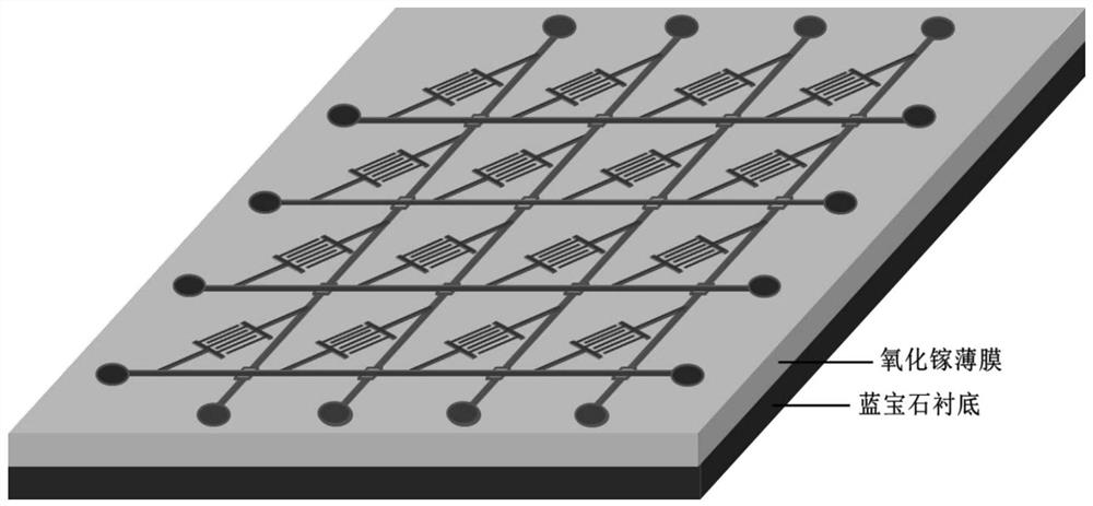
[0047] The present invention provides a β-Ga 2 o 3 The solar-blind ultraviolet photodetector array and its preparation method can make the research on the electrical and photoelectric properties of the detector not limited to a single device, which is beneficial to integration.

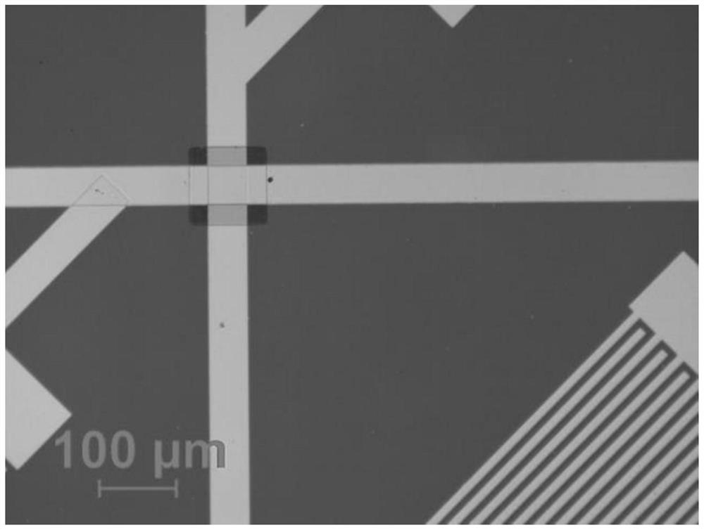
[0048] The detector arrays are layered from bottom to top as follows: β-Ga 2 o 3 Light absorbing layer, lower electrode layer, oxide film insulating layer and upper electrode layer; such as figure 1 As shown, a 4×4 detector array is selected in this embodiment.

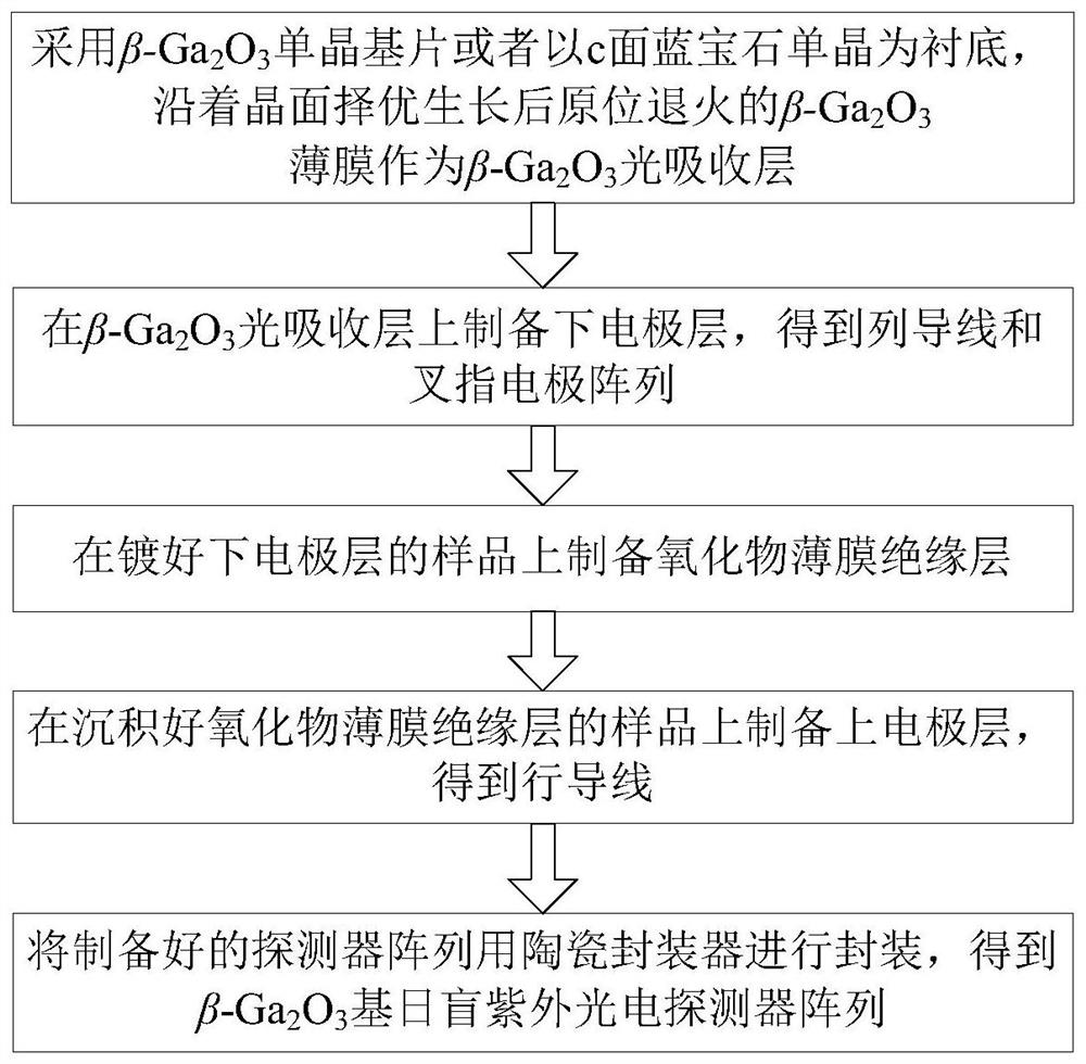
[0049] Using standard semiconductor photolithography process, choose β-Ga as the light absorbing layer 2 o 3 Preparation of β-Ga on a single crystal substrate or on a sapphire substrate by magnetron sputtering, molecular beam epitaxy, pulsed laser deposition or sol-gel 2 o 3 Epitaxial fi...


PUM

PropertyMeasurementUnit
thicknessaaaaaaaaaa
thicknessaaaaaaaaaa
thicknessaaaaaaaaaa

Abstract

The invention discloses a Beta-Ga2O3 based solar-blinded ultraviolet photoelectric detector array and a preparation method thereof, and relates to the photoelectron technical field; the detector array comprises the following structures from bottom to top: a Beta-Ga2O3 luminous absorption layer, a lower electrode layer, an oxide film insulating layer and an upper electrode layer; the Beta-Ga2O3 luminous absorption layer is formed by growing a Beta-Ga2O3 film on a substrate; the lower electrode layer comprising column wires and interdigital electrodes is formed on the Beta-Ga2O3 luminous absorption layer; the oxide film insulating layer is arranged on the lower electrode layer; the most top layer is the upper electrode layer comprising line wires; the oxide film insulating layer is arranged in middle of the intersection portion of the line wires and column wires; the anode of each column of the interdigital electrode is connected on the column wire of the same column; the line wire is connected with the cathode of each line interdigital electrode; the prepared detector array is packaged by a ceramic packaging unit, thus obtaining the Beta-Ga2O3 based solar-blinded ultraviolet photoelectric detector array. The Beta-Ga2O3 based solar-blinded ultraviolet photoelectric detector array is strong in process controllability, low in cost, simple in operation steps, good in repeatability, short in development period, and can be massively produced.

Description

technical field [0001] The invention relates to the field of optoelectronic technology, in particular to a β-Ga 2 o 3 A sun-blind ultraviolet photodetector array and a method of making the same. Background technique [0002] Due to the absorption of the ozone layer, there is almost no deep ultraviolet light with a wavelength between 200-280nm on the surface of the earth. The light in this band is called solar-blind ultraviolet light, and the signal detection for this band is called solar-blind ultraviolet detection. Since it is not affected by the sunlight background, the detection sensitivity of solar-blind ultraviolet light signals is extremely high, and the communication accuracy rate of working in this band is also extremely high. Solar-blind ultraviolet photodetectors can be widely used in scientific research, military, space, environmental protection and other fields, such as ultraviolet light monitors in spaceships, solar ultraviolet monitoring of the ozone layer, t...

Claims


Application Information

Patent Timeline
Patent Type & Authority Patents(China)
IPC IPC(8): H01L31/0224H01L31/102H01L31/18
CPCH01L31/022408H01L31/102H01L31/1828Y02E10/543Y02P70/50
Inventor 唐为华彭阳科
Owner BEIJING UNIV OF POSTS & TELECOMM
Why Eureka
Try Eureka