

Perovskite light emitting diode and preparation method thereof
A technology of perovskite type and perovskite structure, which is applied in semiconductor/solid-state device manufacturing, electrical components, electric solid-state devices, etc., can solve the problems of energy waste and consumption, and achieve the goal of improving device performance and hole injection Effect
- Summary
- Abstract
- Description
- Claims
- Application Information
AI Technical Summary
Problems solved by technology
Method used
Image

Examples
preparation example Construction
[0051] The present invention also provides a method for preparing a perovskite-type electroluminescent device, comprising the following steps:
[0052] (1) Carry out ultrasonic cleaning to substrate layer with ethanol solution, acetone solution and deionized water successively, dry after cleaning;
[0053] (2) transfer the substrate layer to the vacuum chamber to prepare an anode layer;
[0054] (3) Pretreating the substrate of the prepared electrode layer with UV;
[0055] (4) The substrate layer treated in step (3) is sequentially prepared according to the device structure to prepare a functional layer film, and sequentially prepare a hole transport layer, a modification layer, a light-emitting layer and an electron transport layer;
[0056] (5) After the preparation of the functional layer film is completed, the preparation of the cathode layer is carried out in the vacuum evaporation chamber;
[0057] (6) Packaging the device treated in step (5) in a glove box, the glove...
Embodiment 1
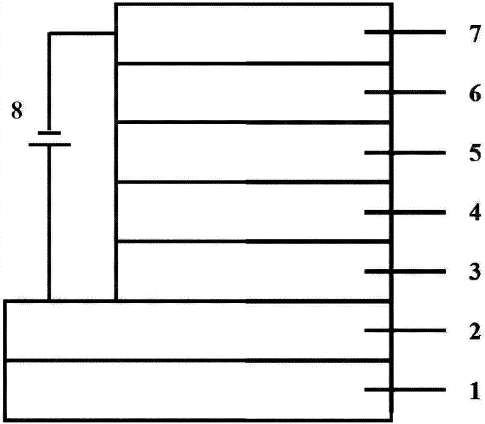
[0060] The device structure is:
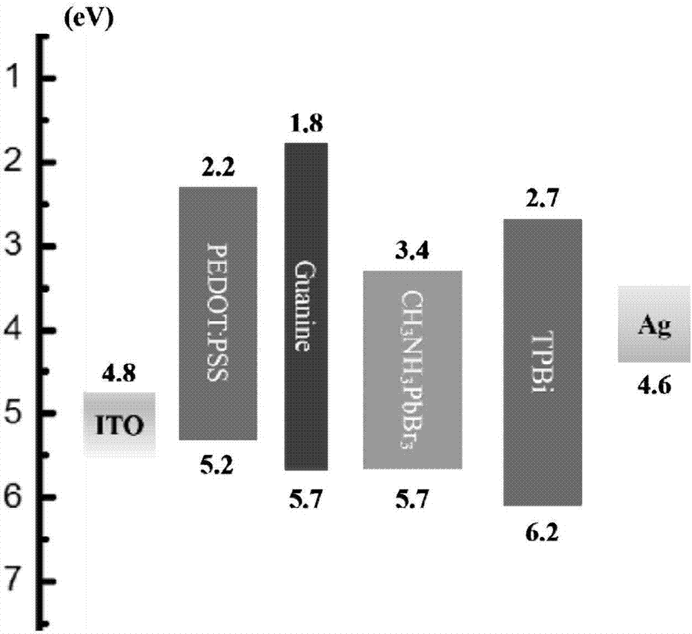
[0061] ITO / PEDOT:PSS(40nm) / guanine(1nm) / CH 3 NH 3 PbBr 3 (50nm) / TPBi(40nm) / Ag(100nm)
[0062] The preparation method is as follows:
[0063] (1) Use ethanol solution, acetone solution and deionized water to ultrasonically clean the transparent conductive substrate ITO glass, and dry it with dry nitrogen after cleaning. The ITO film on the glass substrate is used as the anode layer of the device, and the sheet resistance of the ITO film is 15Ω / □.
[0064] (2) The dried substrate was moved into a vacuum chamber, and the ITO glass was pretreated with ultraviolet and ozone for 10 minutes under an oxygen pressure environment.
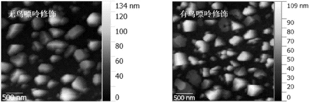
[0065] (3) Spin-coat PEDOT:PSS on the processed substrate, and perform annealing treatment, then move the substrate into a vacuum chamber, evaporate an ultra-thin layer of guanine, control the evaporation rate to 0.01nm / s, and the evaporation rate and The thickness is monitored by a film thickness gauge.
[0066] (4) ...
Embodiment 2
[0072] The device structure is:
[0073] ITO / PEDOT:PSS(40nm) / guanine(2nm) / CH 3 NH 3 PbBr 3 (50nm) / TPBi(40nm) / Ag(100nm)
[0074] The preparation method is as follows:
[0075] (1) Use ethanol solution, acetone solution and deionized water to ultrasonically clean the transparent conductive substrate ITO glass, and dry it with dry nitrogen after cleaning. The ITO film on the glass substrate is used as the anode layer of the device, and the sheet resistance of the ITO film is 15Ω / □.
[0076] (2) The dried substrate was moved into a vacuum chamber, and the ITO glass was pretreated with ultraviolet and ozone for 10 minutes under an oxygen pressure environment.
[0077] (3) Spin-coat PEDOT:PSS on the processed substrate, and perform annealing treatment, then move the substrate into a vacuum chamber, evaporate an ultra-thin layer of guanine, control the evaporation rate to 0.01nm / s, and the evaporation rate and The thickness is monitored by a film thickness gauge.
[0078] (4) ...
PUM
| Property | Measurement | Unit |
|---|---|---|
| Thickness | aaaaa | aaaaa |
| Thickness | aaaaa | aaaaa |
| Thickness | aaaaa | aaaaa |
Abstract
Description
Claims
Application Information