Preparation of columnar granular copper zinc cadmium sulfur (CZCTSSe) thin-film absorption layer and application of layer in solar cell
A copper-zinc-cadmium-tin-sulfur-selenium, columnar grain technology, which can be used in circuits, electrical components, and final product manufacturing, and can solve problems such as many holes
- Summary
- Abstract
- Description
- Claims
- Application Information
AI Technical Summary
Problems solved by technology
Method used
Image
Examples
Embodiment 1
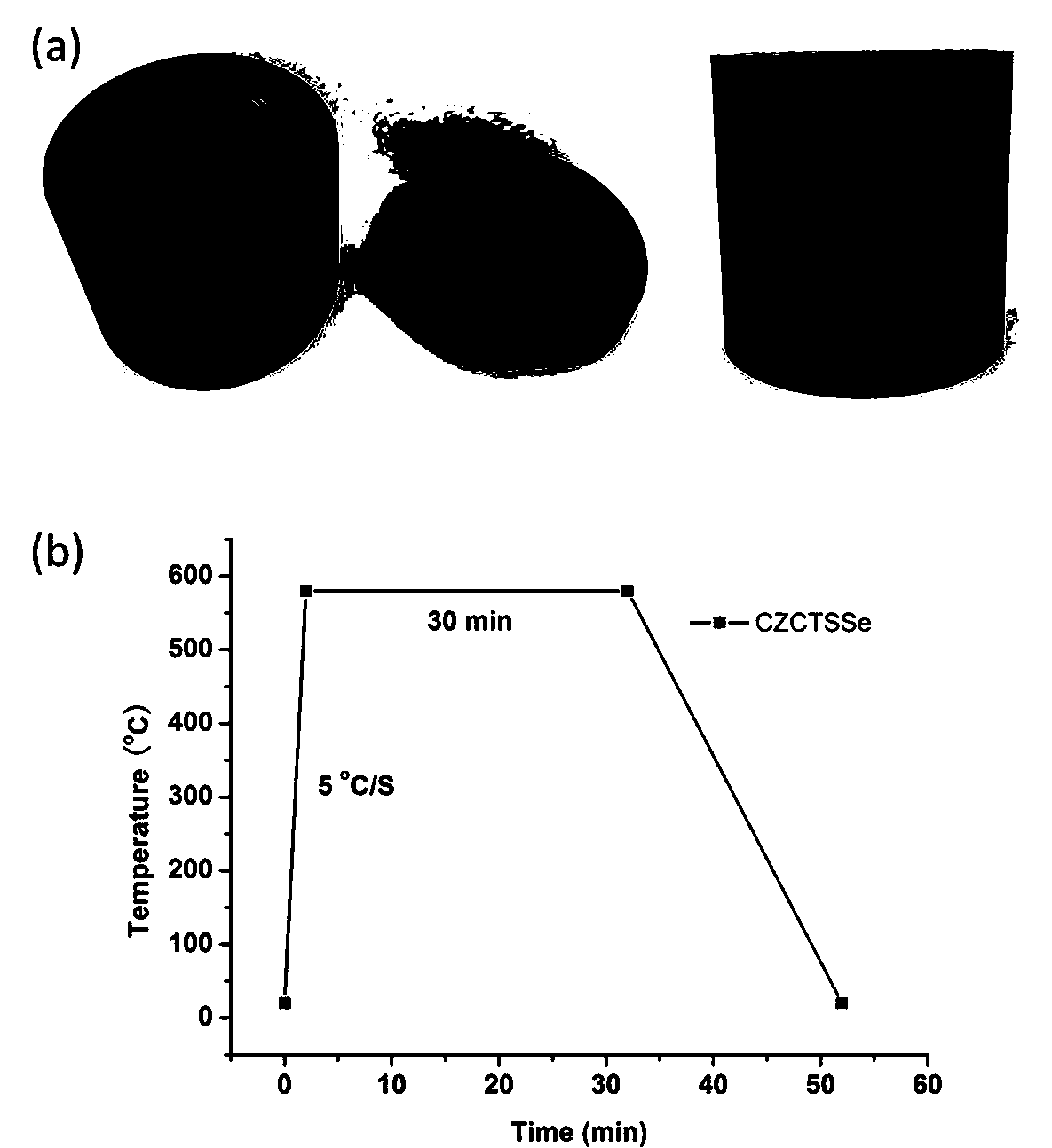
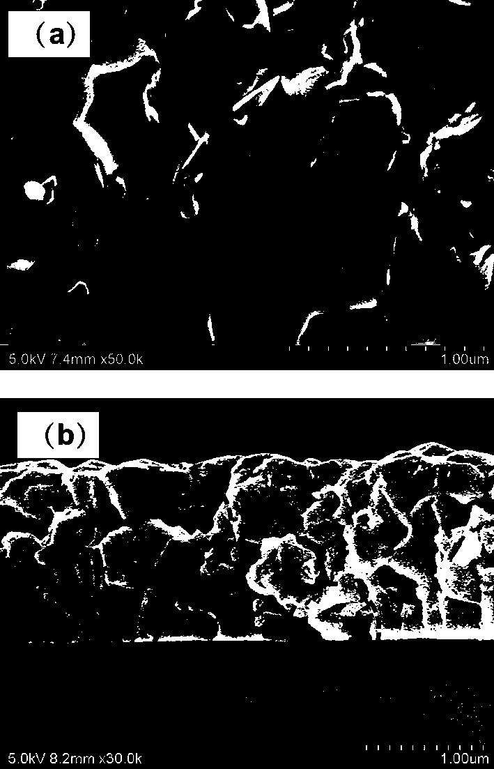
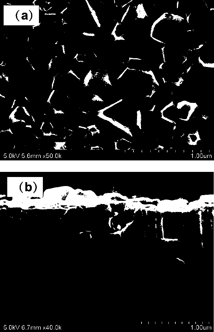
[0023] First prepare pure Cu 2 Zn 1-x Cd x SnS 4 (CZCTS) solution (x=0.05, 18 mL), Cu(AC) 2 2H 2 O(2.48mmol), ZnCl 2 (1.8 mmol), CdCl 2 ·5 / 2H 2 O (0.09 mmol), SnCl 2 2H 2 O (1.5 mmol) and thiourea (8 mmol) were dissolved in 5.5 mL of ethylene glycol methyl ether, and then o C for 1 h to form a brown solution. The pure CZCTS molecular-based solution was spin-coated on a Mo-coated soda-lime glass (SLG) substrate at a rotation speed of 3000 rpm for 20 s. Afterwards, the spin-coated films were subjected to a low-temperature heat treatment for 350 o C, 2 min. The above process was repeated 9 times to prepare a CZCTS precursor film with a thickness of ~1.5 μm. The precursor film was placed in a closed graphite box containing 30 mg for rapid selenization heat treatment. Heat treatment temperature is 580 o C, the holding time is 30 min, and the heating rate is 5 o C / s. Protective atmosphere and pressure: N 2 Gas, 1.1 10 5 Pa. Finally, a granular CZCTSSe absorb...
Embodiment 2
[0026] Take Cu 2 S, ZnS, CdS, SnS 2 as Cu 2 Zn x Cd 1-x SnS 4 Sources of Cu, Zn, Cd, Sn, S; Se powder as Se source. First, mix the above four sulfide powders in a certain proportion, and grind them in an agate mortar for 2-3 hours. After the powder is mixed evenly, at a temperature of 700 o C, Cu with a diameter of 60 mm and a thickness of 3 mm was synthesized by hot pressing at a pressure of 28 Mpa 2 Zn x Cd 1-x SnS 4 Ceramic target. Then, the target was put into the magnetron sputtering vacuum chamber, and the ~1 μm soda-lime glass substrate (SLG / Mo) containing Mo layer was placed directly above the target for thin film deposition. First vacuum the chamber used for sputtering to 7.0 10 -4 Pa, and then pass inert Ar gas and adjust the pressure to 1 Pa (Ar gas flow rate: 30 SCCM). After the pressure is stabilized, start to perform radio frequency magnetron sputtering on the target. Among them, the sputtering power was 60 W, the time was 1 h, and the substrate ...
Embodiment 3
[0029] The granular CZCTSSe obtained in Example 1 is used as the absorbing layer. The device structure of the solar cell refers to the structure of the traditional CZTSSe solar cell: SLG / Mo / CZCTSSe / CdS / i-ZnO / ITO / Al. First, CdS buffer layer (~50 nm) was prepared by chemical bath deposition (CBD) on the selenized CZCTSSe absorbing layer (S1~S5); then, the window layer (~60 nm) was prepared by radio frequency magnetron sputtering. nm i-ZnO, ~250 nm ITO); and the Al electrode (~2μm) was prepared by thermal evaporation; finally, the entire solar cell surface was divided into 9 equal areas (0.16 cm 2 )area.
[0030] The results show that the open circuit voltage of the four copper-based thin film solar cells synthesized under the same conditions is 0.36-0.41 V; the short-circuit current is 23.7-28.2 mA cm 2 ; Conversion efficiency is 3.87% ~ 5.64% (Table 1). It shows that the conversion efficiency of the solar cell is unstable, with large fluctuation and low efficiency.
[003...
PUM
| Property | Measurement | Unit |
|---|---|---|
| Grain size | aaaaa | aaaaa |
| Diameter | aaaaa | aaaaa |
| Size | aaaaa | aaaaa |
Abstract
Description
Claims
Application Information


