

Organic photoelectric detector for image sensor and manufacturing method thereof
A photodetector and image sensor technology, applied in photovoltaic power generation, semiconductor/solid-state device manufacturing, circuits, etc., can solve problems such as narrow spectral response range, and achieve the effects of improving photocurrent, simple process, and expanding spectral response range.
- Summary
- Abstract
- Description
- Claims
- Application Information
AI Technical Summary
Problems solved by technology
Method used
Image

Examples
preparation example Construction
[0041] A method for preparing an organic photodetector for an image sensor of the present invention, specifically comprising the following steps:
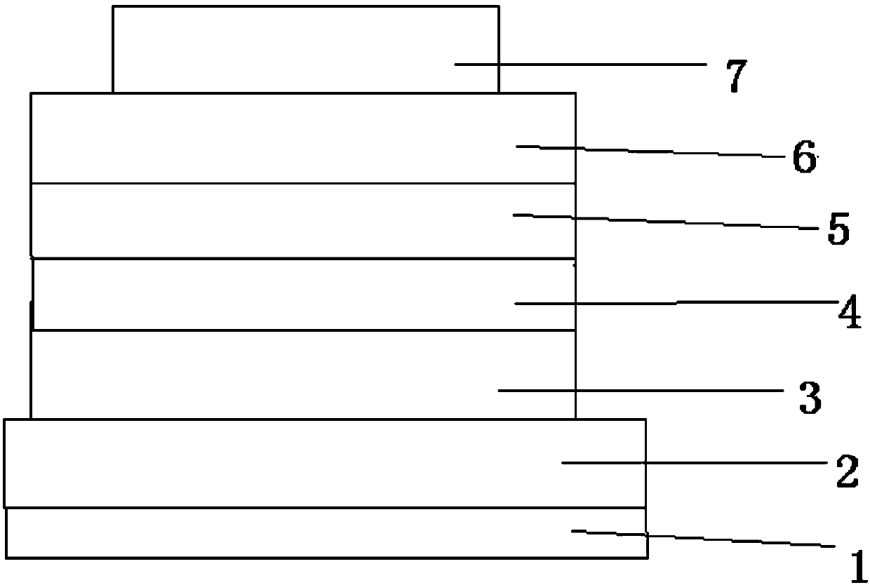
[0042] Step 1: first coat the ITO electrode layer 2 on the glass substrate 1, then use wet method to clean the glass substrate 1 coated with the ITO electrode layer 2, and then dry it with pure nitrogen or infrared;
[0043] The wet cleaning process is as follows:
[0044] Firstly, the glass substrate 1 is ultrasonically cleaned with deionized water for 25 minutes to 35 minutes, then the glass substrate 1 is ultrasonically cleaned with acetone for 25 minutes to 35 minutes, and finally, the glass substrate 1 is ultrasonically cleaned with absolute ethanol for 25 minutes to 35 minutes.
[0045] Step 2: The glass substrate 1 treated in step 1 is cleaned with ultraviolet ozone light, and then placed in a vacuum evaporation chamber to evaporate MoO 3 Layer and NPB layer, form anode buffer layer 3 on glass substrate 1;
[0046] During ...
Embodiment 1
[0059] Step 1: first coat the ITO electrode layer 2 on the glass substrate 1, then use a wet method to clean the glass substrate 1 coated with the ITO electrode layer 2, and dry it with pure nitrogen or infrared;
[0060] The wet cleaning process is as follows:
[0061] Firstly, the glass substrate 1 is ultrasonically cleaned with deionized water for 30 minutes, then the glass substrate 1 is ultrasonically cleaned with acetone for 30 minutes, and finally, the glass substrate 1 is ultrasonically cleaned with absolute ethanol for 30 minutes.
[0062] Step 2: Clean the glass substrate 1 treated in step 1 with ultraviolet ozone light, and then place it in a vacuum evaporation chamber to evaporate MoO 3 Layer and NPB layer, form anode buffer layer 3 on glass substrate 1;
[0063] During the evaporation process, the rotation speed of the turntable carrying the glass substrate 1 is 15r / min, the temperature of the glass substrate 1 is 50°C, and the MoO 3 The evaporation source tempe...
Embodiment 2
[0075] Step 1: first coat the ITO electrode layer 2 on the glass substrate 1, then use a wet method to clean the glass substrate 1 coated with the ITO electrode layer 2, and dry it with pure nitrogen or infrared;
[0076] The wet cleaning process is as follows:
[0077] Firstly, the glass substrate 1 is ultrasonically cleaned with deionized water for 30 minutes, then the glass substrate 1 is ultrasonically cleaned with acetone for 30 minutes, and finally, the glass substrate 1 is ultrasonically cleaned with absolute ethanol for 30 minutes.
[0078] Step 2: Clean the glass substrate 1 treated in step 1 with ultraviolet ozone light, and then place it in a vacuum evaporation chamber to evaporate MoO 3 layer and NPB layer, forming an anode buffer layer 3 on the glass substrate 1;
[0079] During the evaporation process: the rotation speed of the turntable carrying the glass substrate 1 is 15r / min, the temperature of the glass substrate 1 is 50°C, and the MoO 3 The evaporation so...
PUM
| Property | Measurement | Unit |
|---|---|---|
| Thickness | aaaaa | aaaaa |
| Thickness | aaaaa | aaaaa |
| Thickness | aaaaa | aaaaa |
Abstract
Description
Claims
Application Information