
Silicon nanostructured heterojunction solar cell and preparation method thereof

A technology of solar cells and nanostructures, applied in the field of solar cells, can solve the problems of reducing device production costs, reducing lattice order, degrading device performance, etc., achieving reductions in preparation costs and energy consumption, reducing interfacial recombination rates, and device The effect of stability improvement

Inactive Publication Date: 2018-02-16
JILIN NORMAL UNIV
View PDF5 Cites 5 Cited by
  • Summary
  • Abstract
  • Description
  • Claims
  • Application Information

AI Technical Summary

Problems solved by technology

However, the introduction of doping atoms will lead to a decrease in the degree of lattice order, which will increase the bulk defect density of the material, thereby deteriorating the performance of the device; and the introduction of the doping process will also increase the preparation cycle of the device, which is not conducive to reducing the device's performance. production cost; in addition, due to the existence of a large number of dangling bond defects on the surface of silicon nanostructures, when the photogenerated carriers are transported through the heterojunction interface, the high-density dangling bond defects will capture a large number of carriers, which is not conducive to the performance of the device promote

Method used


Image

  • Silicon nanostructured heterojunction solar cell and preparation method thereof
  • Silicon nanostructured heterojunction solar cell and preparation method thereof
  • Silicon nanostructured heterojunction solar cell and preparation method thereof

Examples


Embodiment 1

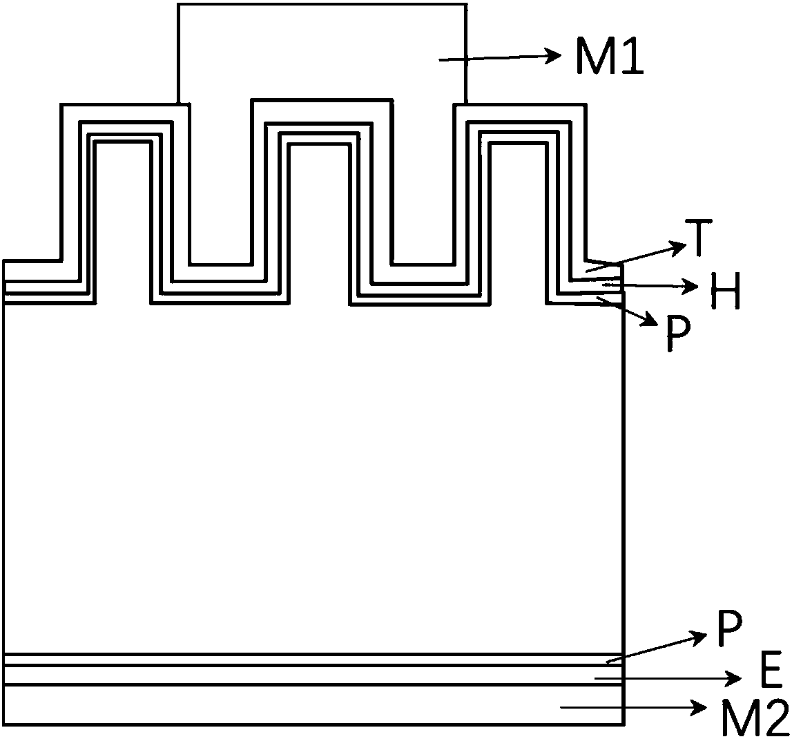
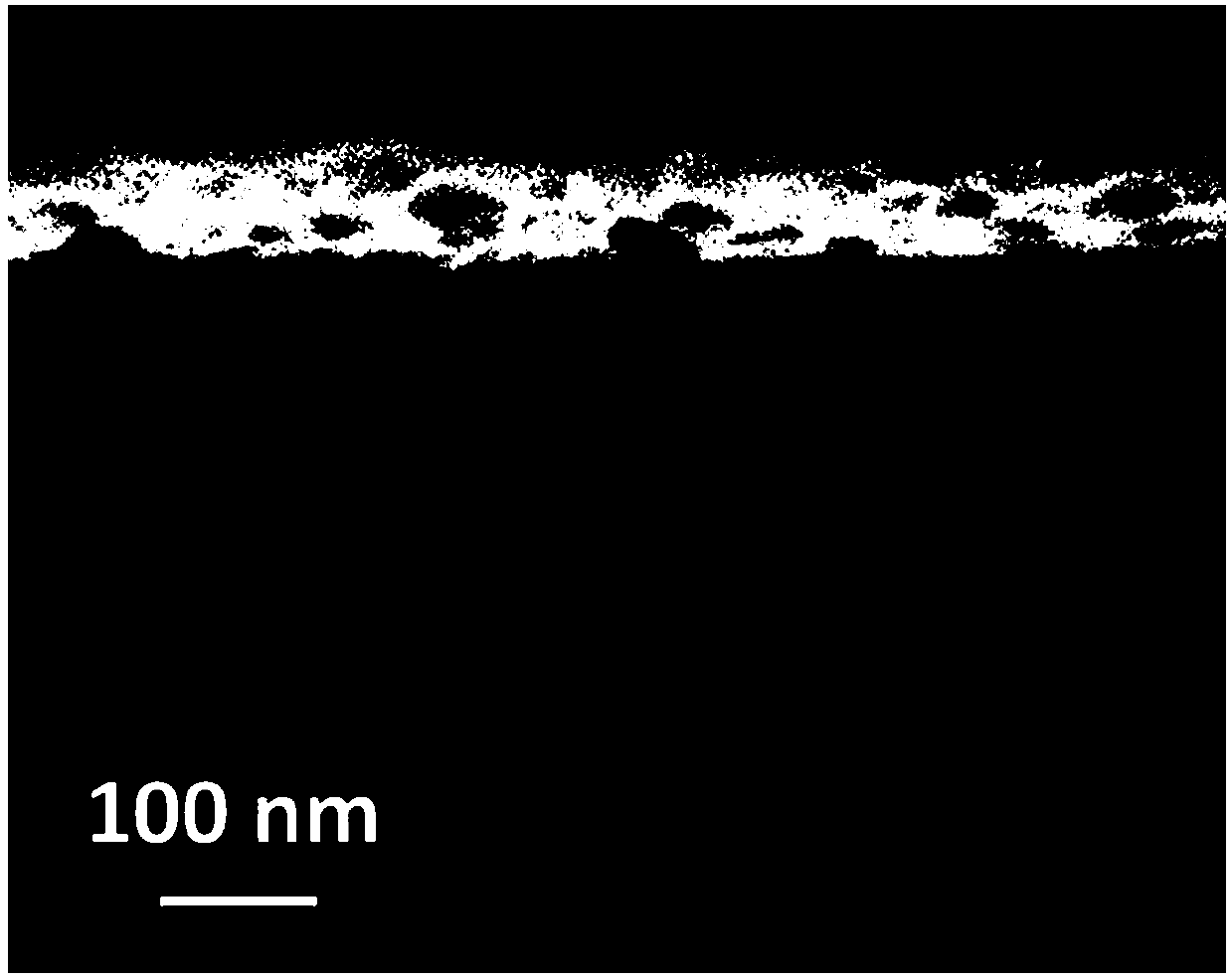
[0029] The structure of a silicon nanostructure heterojunction solar cell in this embodiment is as follows figure 1 As shown, its cross-sectional scanning electron microscope photograph is shown in figure 2 As shown, it includes from top to bottom: metal grid line electrode M1, transparent electrode T, undoped hole transport layer H, ultra-thin silicon oxide passivation layer P, crystalline silicon nanostructure substrate S, ultra-thin silicon oxide Passivation layer P, undoped electron transport layer E and metal back electrode M2.

[0030] The thickness of the ultra-thin silicon oxide passivation layer P is 1.5nm; the transparent electrode T is indium tin oxide with a thickness of 80nm; the undoped hole transport layer H is a molybdenum oxide film with a thickness of 10nm; the undoped electron transport layer E is The cesium carbonate film has a thickness of 2 nm; the crystalline silicon nanostructure substrate S is a single crystal silicon nanowire substrate with a thickn...

Embodiment 2

[0040] The structure of a silicon nanostructure heterojunction solar cell in this embodiment is as follows figure 1 As shown, it includes from top to bottom: metal grid line electrode M1, transparent electrode T, undoped hole transport layer H, ultra-thin silicon oxide passivation layer P, crystalline silicon nanostructure substrate S, ultra-thin silicon oxide Passivation layer P, undoped electron transport layer E and metal back electrode M2.

[0041] The thickness of the ultra-thin silicon oxide passivation layer P is 0.7m; the transparent electrode T is indium tin oxide with a thickness of 80nm; the undoped hole transport layer H is a vanadium oxide film with a thickness of 15nm; the undoped electron transport layer E is The cesium carbonate film has a thickness of 2 nm; the crystalline silicon nanostructure substrate S is a single crystal silicon nanowire substrate with a thickness of 150 μm.

[0042] The silicon nanostructure heterojunction solar cell of this embodiment ...

Embodiment 3

[0051] The structure of a silicon nanostructure heterojunction solar cell in this embodiment is as follows figure 1 As shown, it includes from top to bottom: metal grid line electrode M1, transparent electrode T, undoped hole transport layer H, ultra-thin silicon oxide passivation layer P, crystalline silicon nanostructure substrate S, ultra-thin silicon oxide Passivation layer P, undoped electron transport layer E and metal back electrode M2.

[0052] The thickness of the ultra-thin silicon oxide passivation layer P is 2nm; the transparent electrode T is indium tin oxide with a thickness of 80nm; the non-doped hole transport layer H is a molybdenum oxide film with a thickness of 20nm; The cesium thin film has a thickness of 2 nm; the crystalline silicon nanostructure substrate S is a single crystal silicon nanohole substrate with a thickness of 200 μm.

[0053] The silicon nanostructure heterojunction solar cell of this embodiment is prepared by the following method:

[005...


PUM

PropertyMeasurementUnit
Thicknessaaaaaaaaaa
Thicknessaaaaaaaaaa
Thicknessaaaaaaaaaa

Abstract

The invention provides a silicon nanostructured heterojunction solar cell and a preparation method thereof, and belongs to the technical field of solar cells. The silicon nanostructured heterojunctionsolar cell is composed of a crystalline silicon nanostructured substrate S, an ultra-thin silicon oxide passivation layer P, an undoped hole transport layer H, an undoped electron transport layer E,a transparent electrode T, a metal gate line electrode M1 and a back electrode M2. The effective absorption of incident light is realized by utilizing the high trapping property of the silicon nanostructured substrate. The wide bandgap and high transmission characteristics of the non-doped electron (hole) transport layer are used to further reduce the parasitic absorption of a device and improve the photoelectric conversion efficiency. The electron (hole) transport layer of the silicon nanostructured solar cell does not involve a doping process, and both H and T have the characteristics of high transmission and low parasitic light absorption, the defect state density of the device can be effectively reduced, and the preparation method is simple and easy to implement.

Description

technical field [0001] The invention belongs to the technical field of solar cells. Background technique [0002] With the increasingly prominent environmental problems and the intensification of the energy crisis, solar photovoltaic power generation has developed rapidly because of its safety and reliability, few geographical constraints, and easy integration with buildings. Among many photovoltaic products, silicon nanostructure heterojunction solar cells have attracted widespread attention due to their simple preparation process, abundant raw materials, and high photoelectric conversion efficiency. At present, the conversion efficiency of high-performance silicon nanostructure heterojunction solar cells can reach more than 15%, which has great potential for commercial application. In order to further enhance its application value and expand its application space, it is necessary to reduce the preparation cost while improving the photoelectric conversion efficiency and de...

Claims


Application Information

Patent Timeline
IPC IPC(8): H01L31/0216H01L31/074H01L31/18
CPCH01L31/02167H01L31/074H01L31/1804Y02E10/547Y02P70/50
Inventor 王奉友隋瑛锐魏茂彬范厚刚孙云飞
Owner JILIN NORMAL UNIV
Learn More