
A method and equipment for preparing zno-like crystal thin films

A kind of crystal and equipment technology, applied in the field of preparing ZnO crystal thin film, can solve problems such as difficult mass production, and achieve the effect of strong repeatability, easy operation and strong controllability

Active Publication Date: 2020-03-17
NANJING UNIV OF AERONAUTICS & ASTRONAUTICS
View PDF5 Cites 0 Cited by
  • Summary
  • Abstract
  • Description
  • Claims
  • Application Information

AI Technical Summary

Problems solved by technology

However, at present, the hydrothermal reaction is carried out in a single reactor, which can only perform one-way reaction, and it is difficult to produce in large quantities at the same time

Method used


Image

  • A method and equipment for preparing zno-like crystal thin films
  • A method and equipment for preparing zno-like crystal thin films
  • A method and equipment for preparing zno-like crystal thin films

Examples


Embodiment 1

[0020] (1) Material cleaning: The oxidized Si substrate material on the surface was ultrasonicated for 15 minutes with toluene, acetone, and ethanol respectively, and then rinsed with deionized water; then boiled with aqua regia prepared with concentrated nitric acid and sulfuric acid for 15 minutes; Rinse with hot deionized water and cold deionized water, and dry with nitrogen gas for later use.

[0021] (2) Growth of ZnO seed crystal layer: place the cleaned substrate material in the cavity of the magnetron sputtering equipment, and vacuum up to 8 × 10 -4 pa; the purity of the ZnO ceramic target is 99.99%, the distance between the target and the substrate material is 7cm; the RF sputtering power is 150w, the sputtering time is 1 minute, and the ZnO thickness is about 30nm.

[0022] (3) Solution preparation: 0.2mol Zn(NO 3 ) 2 ▪6H 2 O, 0.02mol HMTA and 0.5mmol Cu(NO 3 ) 2 Dissolve in 100mL deionized water to obtain a mixed solution.

[0023] Growth of ZnO crystal materi...

Embodiment 2

[0025] (1) Material cleaning: The oxidized Si substrate material on the surface was ultrasonicated for 15 minutes with toluene, acetone, and ethanol respectively, and then rinsed with deionized water; then boiled with aqua regia prepared with concentrated nitric acid and sulfuric acid for 15 minutes; Rinse with hot deionized water and cold deionized water, and dry with nitrogen gas for later use.

[0026] (2) Growth of ZnO seed crystal layer: place the cleaned substrate material in the cavity of the magnetron sputtering equipment, and vacuum up to 8 × 10 -4 pa; the purity of the ZnO ceramic target is 99.99%, the distance between the target and the substrate material is 7cm; the RF sputtering power is 150w, the sputtering time is 1 minute, and the ZnO thickness is about 50nm.

[0027] (3) Solution preparation: 0.3mol Zn(NO 3 ) 2 ▪6H 2 O, 0.05mol HMTA and 2mmol Cu(NO 3 ) 2 Dissolve in 100mL deionized water to obtain a mixed solution.

[0028] Growth of ZnO crystal materia...

Embodiment 3

[0030] (1) Material cleaning: The oxidized Si substrate material on the surface was ultrasonicated for 15 minutes with toluene, acetone, and ethanol respectively, and then rinsed with deionized water; then boiled with aqua regia prepared with concentrated nitric acid and sulfuric acid for 15 minutes; Rinse with hot deionized water and cold deionized water, and dry with nitrogen gas for later use.

[0031] (2) Growth of ZnO seed crystal layer: place the cleaned substrate material in the cavity of the magnetron sputtering equipment, and vacuum up to 8 × 10 -4 pa; the purity of the ZnO ceramic target is 99.99%, the distance between the target and the substrate material is 7cm; the RF sputtering power is 150w, the sputtering time is 1 minute, and the ZnO thickness is about 30nm.

[0032] (3) Solution preparation: 0.2molZn(NO 3 ) 2 ▪6H 2 O, 0.04mol HMTA and 5mmol Cu(NO 3 ) 2 Dissolve in 100mL deionized water to obtain a mixed solution.

[0033] Growth of ZnO crystal material...


PUM

PropertyMeasurementUnit
diameteraaaaaaaaaa
thicknessaaaaaaaaaa

Abstract

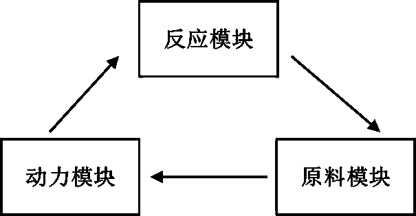
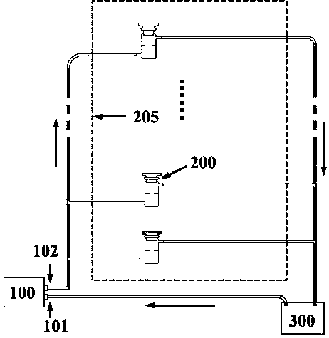
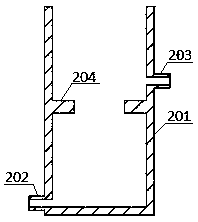
The invention discloses a method and device for preparing a ZnO type crystal thin film and belongs to the field of semiconductor materials with a photoelectric function. According to the method and device for preparing the ZnO type crystal thin film, the ZnO type crystal thin film can be prepared circularly. The method comprises the steps that zinc nitrate, hexamethylene tetramine and copper nitrate are dissolved in deionized water, the concentration ratio of the zinc nitrate to the hexamethylene tetramine to the copper nitrate in an obtained mixed solution is (0.2-0.3 mol): (0.02-0.05 mol): (0.5-5 mol); and a Si substrate material with a grown ZnO seed crystal layer is placed in the mixed solution and reacts at the temperature of 80-100 DEG C. The invention further provides the device forpreparing the ZnO type crystal thin film through a circular array type aqueous solution method. The method and device for preparing the ZnO type crystal thin film have the characteristics that the film thickness is controllable, the device is simple, operation is easy and convenient, the cost is low, and large-batch preparation can be achieved; and meanwhile, the reaction condition is mild, controllability and repeatability are high, and the method and device are suitable for mass production of the ZnO type crystal thin films and achieving industrial application and popularization.

Description

technical field [0001] The invention belongs to the field of photoelectric functional semiconductor materials, and in particular relates to a method and equipment for preparing ZnO crystal thin films. Background technique [0002] ZnO is a new type of Ⅱ-Ⅵ group direct wide bandgap oxide semiconductor material with a wide bandgap at room temperature E g The exciton binding energy is 3.37eV, and the exciton binding energy is 60meV, which is much greater than the thermal ionization energy of 26meV at room temperature. Therefore, the excitons inside ZnO can exist stably at room temperature, so ZnO is a high-efficiency ultraviolet photoelectric suitable for room temperature and higher temperature. Material. ZnO also has excellent piezoelectricity, gas sensitivity, pressure sensitivity and humidity sensitivity, and excellent electromechanical coupling performance. It has been widely studied and used in various optoelectronic devices such as photodetectors, light-emitting diodes...

Claims


Application Information

Patent Timeline
Patent Type & Authority Patents(China)
IPC IPC(8): C23C18/12C23C14/08C23C28/04
CPCC23C14/086C23C18/1216C23C28/04
Inventor 徐强李子奕
Owner NANJING UNIV OF AERONAUTICS & ASTRONAUTICS
Learn More