Precise wire circuit and preparation method thereof

A kind of wire line, fine technology, applied in the direction of printed circuit manufacturing, printed circuit, conductive pattern formation, etc., can solve the problems of resource consumption, waste water pollution, time-consuming etching, etc., to achieve the effect of improving production efficiency

Active Publication Date: 2018-02-23
GUANGDONG GUANGHUA SCI TECH
View PDF4 Cites 2 Cited by
  • Summary
  • Abstract
  • Description
  • Claims
  • Application Information

AI Technical Summary

Problems solved by technology

These processes not only have a long process, but also cause a large amount of waste water to pollute the environment and consume a large amount of resources. Based on this situation, a method of making metal circuits by laser direct writing technology is proposed.
[0003] The current subtractive, semi-additive, and full-additive methods of HDI boards or packaging substrates have long processes, exposure, development, and etching time-consuming and material-consuming defects.

Method used


Image

  • Precise wire circuit and preparation method thereof
  • Precise wire circuit and preparation method thereof

Examples


preparation example Construction

[0030] A method for preparing a fine conductive circuit, comprising the steps of:

[0031] Step 1: configure the slurry, the slurry includes metal ions and reducing agents; it can be understood that it can also include viscosity modifiers, antioxidants and solvents;

[0032] Step 2: performing surface treatment on the substrate material to be coated with slurry to enhance the bonding force between the substrate material and the metal wire (optional step);

[0033] Step 3: irradiate the slurry with laser to make the reducing agent react with metal ions to form fine lines;

[0034] Step 4: cleaning and removing the unreacted slurry;

[0035] Step 5: Thicken the formed fine circuit by electroplating or electroless plating to form a final circuit pattern (an optional step).

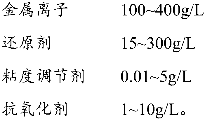
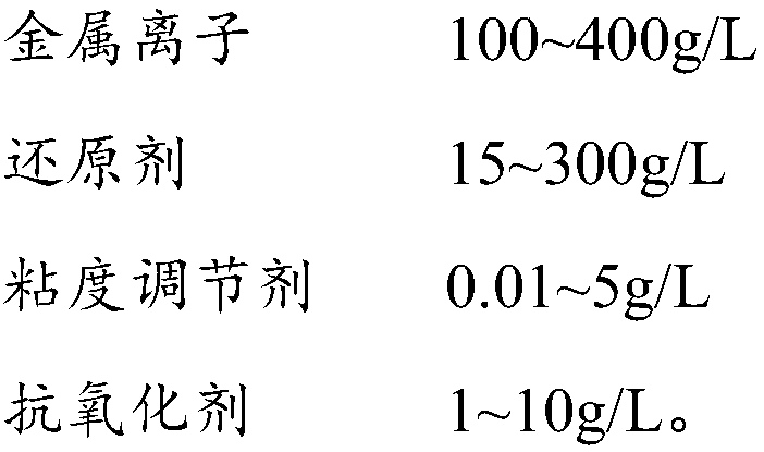
[0036] The slurry in step 1 mainly comprises metal ion compound, reducing agent and auxiliary materials such as viscosity regulator, antioxidant and solvent.

[0037] The metal ions comprise the following ...

Embodiment 1

[0051] Use the mixed slurry of copper acetate monohydrate and acetic acid to make fine wire lines, and the specific steps are as follows:

[0052] (1) Use copper acetate monohydrate, acetic acid to mix and add methylcellulose aqueous solution to form a slurry (viscosity is 10.2Pa s): copper acetate monohydrate 620g / L, acetic acid 130g / L, hydroxymethylcellulose 8g / L, antioxidant (ascorbic acid) 10g / L;

[0053] (2) Use sodium hydroxide to treat the surface of the glass substrate and perform ultrasonic heating treatment for 30 minutes;

[0054] (3) Spread the slurry evenly on the glass substrate (the thickness of the slurry is about 100 μm), and irradiate with laser to form a circuit (the laser spot diameter is 500nm-50μm, and the laser wavelength range is 193nm-1650nm);

[0055] (4) drying the glass substrate, and cleaning off excess slurry;

[0056] (5) Use tape to stick the line part and tear it off, and no powder is found.

Embodiment 2

[0058] Use titanium acetylacetonate and ethanol to make fine wire circuits to form a circuit with titanium as a flexible base material. The specific steps are as follows:

[0059] (1) Use titanium acetylacetonate and ethanol and isopropanol and water to mix to form a slurry (viscosity is 9.52Pa s): titanium acetylacetonate 260g / L, reducing agent ethanol and isopropanol are 50 and 60g / L respectively, viscosity Regulator (hydroxymethylcellulose) 10g / L, antioxidant (ascorbic acid) 15g / L;

[0060] (2) Use plasma to treat the PI flexible base material, and rinse with water;

[0061] (3) Spread the slurry evenly on the PI substrate (the thickness of the slurry is about 100 μm), and irradiate with laser to form a circuit;

[0062] (4) Remove excess slurry on the substrate.


PUM

PropertyMeasurementUnit
diameteraaaaaaaaaa
wavelengthaaaaaaaaaa

Abstract

The invention relates to a precise wire circuit and a preparation method thereof. The preparation method comprises the following steps of (1) preparing paste, wherein the paste comprises metal ions and a reducing agent; (2) laying the paste on a surface of a substrate; (3) irradiating the paste with laser, and reducing the metal ions to elemental metal so as to form a circuit; and (4) cleaning thepaste which is not reacted, and obtaining the precise wire circuit. According to the preparation method (direct-writing technology) of the precise wire circuit, a method for forming the circuit or aconductive pattern through chemical or photochemical reaction between the substrate and the paste by means of an optical effect or a heat effect of the laser on a surface of the substrate and the paste is employed, the direct-writing technology is high in accuracy, a mask is not needed, and the direct-writing technology is applicable to an arbitrary substrate.

Description

technical field [0001] The invention relates to the field of electronic component manufacturing, in particular to a fine wire circuit and a preparation method thereof. Background technique [0002] With the popularity of the network and the rapid development of electronic communications, electronic terminal products are required to continuously improve their product performance and at the same time require their miniaturization, and high-density interconnection technology (HDI) has emerged as the times require. HDI technology refers to coating an insulating medium on an insulating substrate or a traditional printed circuit board, forming lines and vias through electroless plating and electroplating, and finally forming a multilayer printed circuit board through multiple stacking. The traditional methods of making HDI mainly include subtractive method and additive method. Among them, the subtractive method, also known as the copper etching method, is a method of selectively ...

Claims


Application Information

Patent Timeline
Patent Type & Authority Applications(China)
IPC IPC(8): H05K3/10C09D101/28C09D189/06C09D105/12C09D7/63C08J7/04C23C18/14
CPCC08J7/0427C08J2355/02C08J2363/00C08J2379/08C08J2401/28C08J2405/12C08J2489/06C08K5/05C08K5/09C08K5/098C08K5/13C08K5/1535C08K5/56C09D101/28C09D101/284C09D105/12C09D189/06C23C18/14H05K3/105H05K2203/107
Inventor 郑莉王翀梁坤程骄肖定军
Owner GUANGDONG GUANGHUA SCI TECH
Why Eureka
Try Eureka