Enhanced graphene-silicon heterojunction photoelectric detection chip and preparation method thereof

A photoelectric detection and silicon heterojunction technology, which is applied in photovoltaic power generation, circuits, electrical components, etc., can solve the problems of large limitations in the control of element types and content, lack of control means for response rate, and insignificant advantages in photoresponsivity. Achieve the effects of increasing the local optical field density, expanding the spectral selection characteristics, and increasing the light response rate

Inactive Publication Date: 2018-03-06
XIAMEN UNIV
View PDF5 Cites 13 Cited by
  • Summary
  • Abstract
  • Description
  • Claims
  • Application Information

AI Technical Summary

Problems solved by technology

With the rapid development of the field of electronic information, this kind of material faces many limitations in the preparation of high-performance detection chips: for example, the doping concentration in a single semiconductor is limited by the solid solubility of the material itself, and the types of elements and the The control of the content is limited, the process is complicated, and it is difficult to integrate with the silicon base, etc.
However, the current graphene-silicon heterojunction photodetection chip has no obvious advantages in photoresponsivity (generally on the order of 0.5A / W), and there is still a lack of effective control methods for response rate improvement and specific spectral enhancement.

Method used


Image

  • Enhanced graphene-silicon heterojunction photoelectric detection chip and preparation method thereof
  • Enhanced graphene-silicon heterojunction photoelectric detection chip and preparation method thereof
  • Enhanced graphene-silicon heterojunction photoelectric detection chip and preparation method thereof

Examples


Embodiment

[0040] Embodiment: Preparation of enhanced graphene-silicon heterojunction photodetection chip:

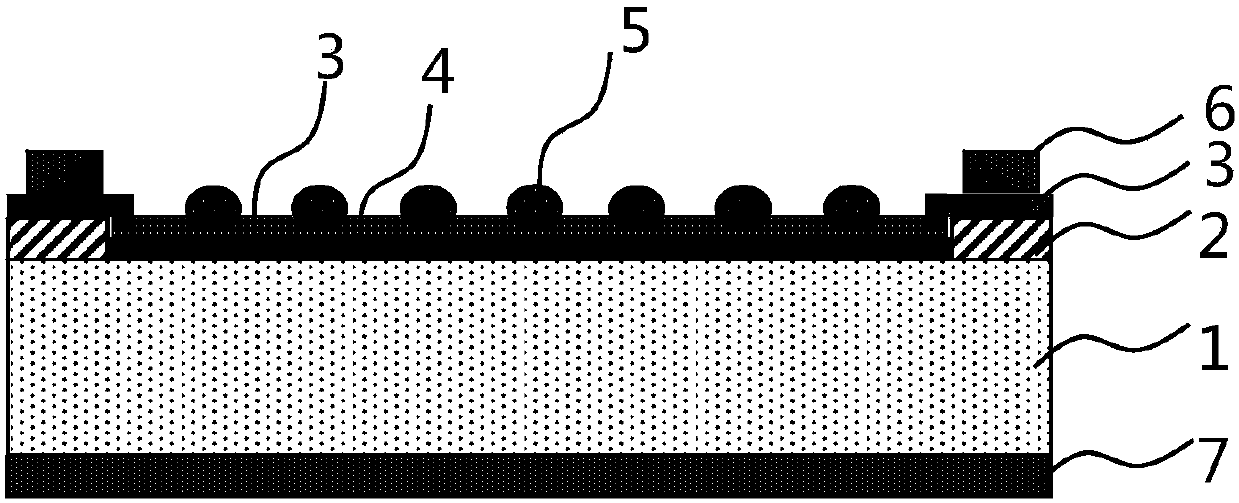
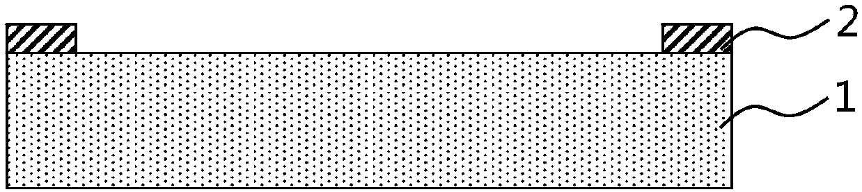
[0041] S1. First, clean the 4-inch N-type silicon substrate with RCA standard, and then oxidize the surface of the silicon wafer in a thermal oxidation furnace. The thickness of the oxide layer is 300nm; Ultrasonic cleaning in water for 20 minutes;

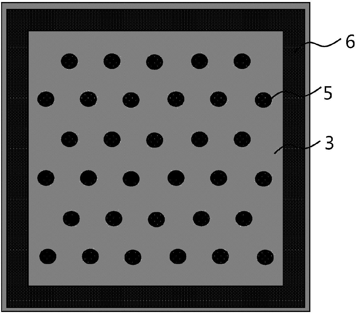
[0042] S2. Perform photolithography on the cleaned silicon wafer, and prepare an array-type window pattern area on the front surface of the silicon wafer; after development, the window area is exposed; the wafer after development and post-baking is etched in BOE solution for 2 minutes, Removal of SiO in window area and backside 2 layer; after removing the glue, the N-type silicon is exposed in the front window area of ​​the wafer, which is the light-absorbing active area of ​​the subsequent photodetection chip, such as image 3 As shown, where the window area is surrounded by unetched SiO 2 Floor;

[0043] S3. Place the wafer that...


PUM

PropertyMeasurementUnit
electrical resistivityaaaaaaaaaa
thicknessaaaaaaaaaa
thicknessaaaaaaaaaa

Abstract

The invention discloses a graphene-silicon heterojunction photoelectric detection chip and a preparation method thereof. The detection chip includes a silicon substrate, a frame-shaped SiO2 insulatinglayer on the boundary around the silicon substrate, an interface passivation layer on the silicon substrate, a graphene layer on the interface passivation layer, and a metal nanostructure layer on the graphene layer. By introducing the metal nanostructure to the chip structure, on one hand, the light absorption efficiency of the graphene-silicon heterojunction can be significantly improved and the light responsivity and linear light response range of devices can be improved through the localized surface plasmon resonance characteristic of the metal nanostructure. On the other hand, through the ultrafast photoelectric conversion process of the metal nanostructure under light excitation, the spectral response rate and frequency characteristic of the chip can be significantly improved. In addition, by making use of different spectrum resonance characteristics of metal nanoparticles of different materials and sizes, the specific spectrum enhancement characteristic of the detection chip can be significantly improved.

Description

technical field [0001] The invention belongs to the field of optoelectronic technology, and in particular relates to a graphene-silicon heterojunction photodetection chip and a manufacturing method thereof. Background technique [0002] A photodetector chip is a medium that obtains optical information by converting optical signals into electrical signals. Due to the advantages of small size, low power consumption, and high sensitivity, photoelectric detection chips have been used in various fields of people's lives, especially in recent years. The broadest class of electronic devices. [0003] Traditional photodetection chips are mainly based on PN or PIN structures of semiconductor materials such as silicon, germanium, and gallium arsenide, and the detection spectral band can cover ultraviolet to far infrared bands. With the rapid development of the field of electronic information, this kind of material faces many limitations in the preparation of high-performance detecti...

Claims


Application Information

Patent Timeline
Patent Type & Authority Applications(China)
IPC IPC(8): H01L31/0216H01L31/109H01L31/18
CPCH01L31/02161H01L31/109H01L31/1804Y02E10/547Y02P70/50
Inventor 尹君李静应安妮刘恋
Owner XIAMEN UNIV
Why Eureka
Try Eureka