
A kind of mosfet device nitriding method

A device and nitriding treatment technology, which is applied in the direction of semiconductor devices, semiconductor/solid-state device manufacturing, electrical components, etc., can solve the problem that the interface state density cannot be sufficiently reduced, the reliability of SiO gate dielectric is reduced, and the nitriding passivation effect is reduced, etc. problems, avoiding the reduction of reliability and breakdown electric field strength, avoiding the risk of potential toxicity and poisonous gas leakage, and simplifying the effect of nitriding passivation gas system

Active Publication Date: 2021-05-07
ZHUZHOU CRRC TIMES SEMICON CO LTD
View PDF6 Cites 0 Cited by
  • Summary
  • Abstract
  • Description
  • Claims
  • Application Information

AI Technical Summary

Problems solved by technology

[0007] 1) Different gases need to be used for multi-step nitriding passivation, and the process is complicated;
[0008] 2) NO is a poisonous gas; N 2 The decomposition of O at high temperature will also produce toxic gas NO; NH 3 Flammable, Toxic, Irritant
Therefore, the annealing equipment has high sealing requirements, expensive equipment, and needs to be equipped with a complex tail gas treatment system, the process is dangerous and the process cost is high
[0009] 3) NO and N 2 O itself is oxidizing, and when N atoms are introduced at the interface, it will also oxidize SiO 2 The / SiC interface is further oxidized, resulting in the generation of new interface traps, and the interface state density cannot be sufficiently reduced, thereby reducing the effect of nitriding passivation;
[0010] 4) NH 3 Passivation also introduces excess N atoms throughout the dielectric, resulting in SiO 2 The breakdown electric field strength of the dielectric is significantly reduced, reducing the SiO 2 Gate Dielectric Reliability

Method used


Image

  • A kind of mosfet device nitriding method
  • A kind of mosfet device nitriding method
  • A kind of mosfet device nitriding method

Examples


Embodiment approach

[0063] According to a preferred embodiment of the present invention, the method further includes: after the oxidation treatment and nitriding treatment, annealing the MOSFET device in an inert gas atmosphere, and then lowering the temperature in an inert gas atmosphere; the preferred annealing temperature is 1200-1500 ℃, the annealing time is 30-120 minutes. The annealing treatment of this step does not contain N 2 Inert atmosphere, such as Ar atmosphere. Further inert gas treatment favors the release of SiO 2 Impurities in the medium improve the compactness of the oxide film.

[0064] Then, the temperature was naturally lowered to room temperature in an inert gas atmosphere without N2, and finally the SiO 2 dielectric SiC epitaxial wafers. Natural cooling in an inert gas atmosphere that does not contain N2 avoids N during the cooling process 2 with SiO 2 Unstable reactions at the / SiC interface, thereby affecting the SiO 2 / SiC interface quality.

[0065] According to...

specific Embodiment 1

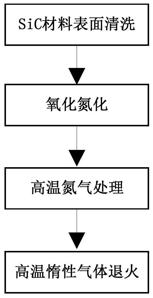
[0074] use as image 3 The operation process shown is to clean the SiC epitaxial wafer of the SiC MOSFET device, perform high-temperature oxidative nitriding treatment, high-temperature nitriding treatment, annealing, and cooling treatment.

[0075] 1) SiC epitaxial wafer cleaning

[0076] The SiC epitaxial wafer of the SiC MOSFET device is cleaned by the RCA cleaning process using SPM solution, APM solution, HPM solution and HF solution (the specific conditions are as above, and the details of the cleaning operation are not described here), and the surface of the SiC epitaxial wafer is removed. Contaminants such as organic matter, particles and metal impurities that may be present.

[0077] 2) SiC epitaxial wafer oxidation and nitriding treatment

[0078] The SiC epitaxial wafer cleaned by RCA was placed in a vertical oxidation furnace, and the temperature was raised to 1350°C, the heating rate was 10°C / min, the gas atmosphere was Ar, and the pressure in the furnace tube wa...

specific Embodiment 2

[0089] 1) SiC epitaxial wafer cleaning

[0090] The SiC epitaxial wafer of the SiC MOSFET device is cleaned by the RCA cleaning process, using SPM solution, HF solution, APM solution and HPM solution to remove the organic matter, particles and metal impurities that may exist on the surface of the SiC epitaxial wafer.

[0091] 2) SiC epitaxial wafer oxidation treatment

[0092] The SiC epitaxial wafer cleaned by RCA was placed in a vertical oxidation furnace, and the temperature was raised to 1350°C, the heating rate was 10°C / min, the gas atmosphere was Ar, and the pressure in the furnace tube was 800mbar.

[0093] After the temperature of the furnace tube of the oxidation furnace is stabilized at the set oxidation temperature, the oxidizing gas (O 2 and H 2 ).

[0094] 3) High temperature nitrogen treatment

[0095]After the oxidation process is completed, the oxidizing gas is turned off, and N is introduced into the furnace tube at a rate of 2.0 slm. 2 , in pure N 2 Ann...


PUM


Abstract

The present invention provides a method for nitriding a MOSFET device, comprising nitriding the MOSFET device with nitrogen-containing gas, preferably the nitriding treatment is performed at a temperature of 1200-1500°C, preferably 1250-1450°C. According to the nitriding method of the power device provided by the present invention, nitrogen is used for nitriding at a high temperature during the oxidation process and / or after oxidation of the device, which simplifies the nitriding passivation gas system, avoids gate dielectric reliability and breakdown electric field strength The reduction of potential toxicity and poisonous gas leakage risk caused by nitriding gas is avoided, and the exhaust gas treatment system is simplified.

Description

technical field [0001] The invention relates to the field of power devices, in particular to a nitriding and passivation method for a MOSFET device. Background technique [0002] SiC material is currently the only one that can form SiO through thermal oxidation 2 The compound semiconductor of the film, which makes the manufacture and performance optimization of SiCMOSFET (Metal-Oxide-Semiconductor Field-Effect Transistor, Metal-Oxide-Semiconductor Field-Effect Transistor) devices can learn from the mature Si process. However, SiC MOSFET devices suffer from low channel mobility, mainly due to the thermal oxidation of SiO 2 / SiC interface state density is too high. SiO 2 / SiC interface state traps mainly originate from near-interface defects in the oxide layer and SiO 2 Carbon residue at the / SiC interface. Since the SiC lattice contains carbon atoms, there are carbon dangling bonds or carbon clusters remaining at the interface after thermal oxidation. These interface st...

Claims


Application Information

Patent Timeline
Patent Type & Authority Patents(China)
IPC IPC(8): H01L21/336H01L21/223
CPCH01L21/223H01L29/66477
Inventor 王弋宇李诚瞻吴佳史晶晶高云斌陈喜明赵艳黎吴煜东刘可安
Owner ZHUZHOU CRRC TIMES SEMICON CO LTD
Learn More