Aluminium nitride single crystal growth device dispensing with seed crystal bonding technology and method

A growth device, aluminum nitride technology, applied in the direction of single crystal growth, single crystal growth, crystal growth, etc., can solve the problem of uneven temperature field distribution on the surface of the seed crystal, few types of non-carbon high-temperature adhesives, affecting the single crystal problems such as usable area, to achieve the effect of simple device and process method, increase usable area, and eliminate cracks

Active Publication Date: 2018-03-23
PEKING UNIV
View PDF14 Cites 13 Cited by
  • Summary
  • Abstract
  • Description
  • Claims
  • Application Information

AI Technical Summary

Problems solved by technology

However, there are few types of non-carbon-containing high-temperature adhesives, the price is expensive, and the bonding effect is obviously inferior to carbon-containing adhesives;
[0005] (2) The seed crystal bonding technology has strict requirements on the process, and the uneven coating and solidification process is easy to form micropores, and the difference in thermal conductivity will lead to uneven distribution of the temperature field on the surface of the seed crystal, which will affect the usable area of ​​​​the single crystal;
[0006] (3) Once the bonding is not firm, it is easy to cause the seed crystal to fall off during the growth process and lead to the failure of the entire experiment and many other problems.
[0007] It can be seen that the traditional method of bonding seed crystals in the physical vapor transport method is likely to affect the quality of the aluminum nitride single crystal produced, so there is an urgent need for an aluminum nitride single crystal growth device and a method for growing aluminum nitride single crystals without seed crystal bonding technology. craft

Method used


Image

  • Aluminium nitride single crystal growth device dispensing with seed crystal bonding technology and method
  • Aluminium nitride single crystal growth device dispensing with seed crystal bonding technology and method
  • Aluminium nitride single crystal growth device dispensing with seed crystal bonding technology and method

Examples


Embodiment 1

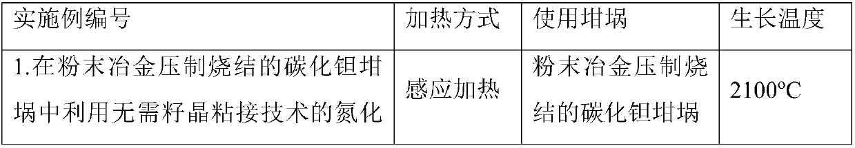
[0047] Embodiment 1: In a tantalum carbide crucible sintered by powder metallurgy, the growth of high-purity single crystal aluminum nitride is accomplished by using an aluminum nitride single crystal growth device that does not require seed crystal bonding technology.

[0048] The specific growth process is as follows:

[0049] (1) The induction coil feeds a current to heat the graphite.

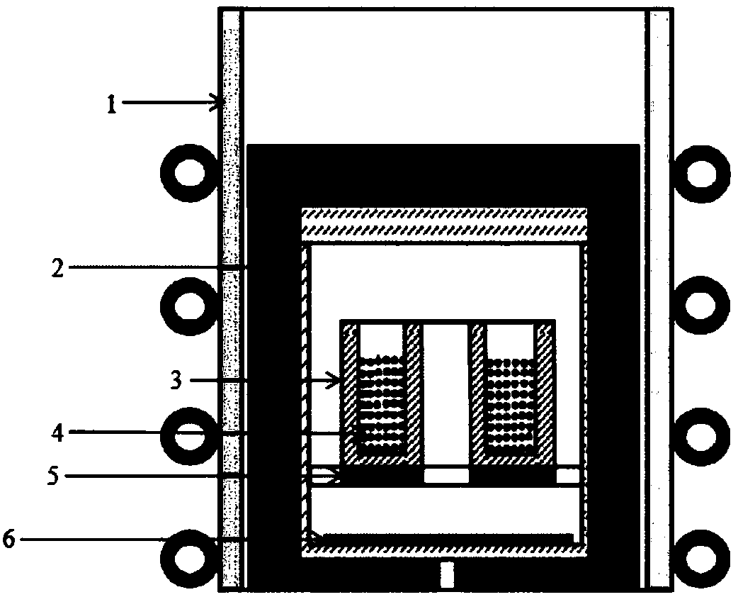
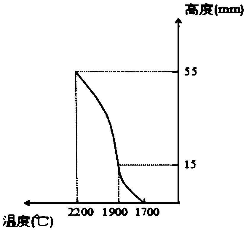
[0050] (2) Adjust the structure of the insulation layer so that the thickness of the top insulation material is greater than that of the bottom, so that the temperature at the top of the crucible is about 400°C higher than the temperature at the bottom. At the same time, an opening with a diameter of 9 mm is left directly below to ensure that the infrared temperature measurement system can perform non-contact infrared measurement of the thermal field conditions at the bottom of the crucible.

[0051] (3) The crucible is a tantalum carbide ceramic crucible sintered with tantalum carbide pow...

Embodiment 2

[0057] Embodiment 2: The growth of high-purity single-crystal aluminum nitride is completed in a carbonized metal tantalum crucible using an aluminum nitride single crystal growth device that does not require seed crystal bonding technology.

[0058] The specific growth process is as follows:

[0059] (1) The induction coil feeds a current to heat the graphite.

[0060] (2) Adjust the structure of the insulation layer so that the thickness of the top insulation material is greater than that of the bottom, so that the temperature at the top of the crucible is about 400°C higher than the temperature at the bottom. At the same time, an opening with a diameter of 9 mm is left directly below to ensure that the infrared temperature measurement system can perform non-contact infrared measurement of the thermal field conditions at the bottom of the crucible.

[0061] (3) The crucible is a tantalum crucible with a carbonized tantalum surface. The size of the carbonized tantalum crucib...

Embodiment 3

[0067] Embodiment 3: The growth of high-purity single-crystal aluminum nitride is completed in a tungsten crucible by using an aluminum nitride single crystal growth device that does not require seed crystal bonding technology.

[0068] The specific growth process is as follows:

[0069] (1) Pass current through the high-purity tungsten mesh (resistance heating) to heat it.

[0070] (2) Multi-section high-purity tungsten screens are used as the insulation layer, and the structure (shape and number of layers) of the insulation layer is adjusted so that the insulation effect of the top is greater than that of the bottom, and the temperature at the top of the crucible is about 400°C higher than that at the bottom. At the same time, an opening with a diameter of 9 mm is left directly below to ensure that the infrared temperature measurement system can perform non-contact infrared measurement of the thermal field conditions at the bottom of the crucible.

[0071] (3) The crucible ...


PUM

PropertyMeasurementUnit
diameteraaaaaaaaaa
diameteraaaaaaaaaa
heightaaaaaaaaaa

Abstract

The invention discloses an aluminium nitride single crystal growth device dispensing with a seed crystal bonding technology and a process and relates to the semiconductor manufacture technology. The aluminium nitride single crystal growth device comprises a heating system, an infrared temperature measurement system, seed crystals, a growth crucible, a crucible partition and a double-layered nestedcrucible, wherein the heating system is arranged on the outermost side; a temperature difference exists between the bottom and the top of the crucible; the crucible is arranged in a heat insulation material; the seed crystals are placed at the bottom of the crucible; the double-layered nested crucible is vertically placed on the upper side of the crucible partition and comprises an inner-layer crucible and an outer-layer crucible; the heights of the walls of the inner-layer crucible and the outer-layer crucible are kept the same; and a gap between the side walls of the inner-layer crucible and the outer-layer crucible is filled with high-purity aluminium nitride powder. Doping of aluminium nitride single-crystal impurity elements can be reduced, the crystal quality is improved, the single-crystal usable area is increased, the aluminium nitride single crystal growth device is simple and easy to use, facilitates low-cost preparation of aluminium nitride single crystals, and can preventgrowth of the aluminium nitride single crystals from being influenced by the seed crystal bonding technology.

Description

technical field [0001] The invention relates to a semiconductor manufacturing device and a process, in particular to an aluminum nitride (AlN) single crystal growth device and a process method without seed crystal bonding technology. Background technique [0002] The bandgap width of the third-generation semiconductor materials is generally greater than 3.0 electron volts, so it is also called a wide bandgap semiconductor, and aluminum nitride materials belong to it. It has high thermal conductivity, high breakdown field strength, and high saturation electron drift rate. Excellent properties such as high bonding energy and high bonding energy have great application prospects in high-temperature, high-frequency, high-power and radiation-resistant devices. The research and development of aluminum nitride single crystal materials has become a hot spot in the semiconductor field. Currently, the method of physical vapor transport (PVT) is mainly used to prepare aluminum nitride s...

Claims


Application Information

Patent Timeline
Patent Type & Authority Applications(China)
IPC IPC(8): C30B23/02C30B29/40
CPCC30B23/02C30B29/403
Inventor 吴洁君朱星宇程玉田李孟达韩彤于彤军张国义
Owner PEKING UNIV
Why Eureka
Try Eureka