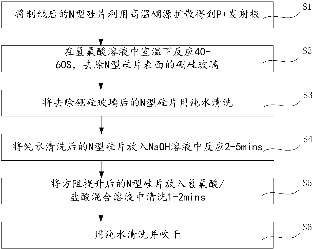
Boron diffusion method for N-type solar cell
A solar cell and diffusion method technology, which is applied in the field of solar cell preparation technology, can solve the problem of low concentration of boron atoms, achieve the effects of optimizing ohmic contact, reducing junction depth, and improving conversion efficiency
- Summary
- Abstract
- Description
- Claims
- Application Information
AI Technical Summary
Problems solved by technology
Method used
Image
Examples
Embodiment 1
[0032] This embodiment provides a boron diffusion method for an N-type solar cell, comprising the following steps:
[0033] S1: The N-type silicon wafer after texturing is diffused by a high-temperature boron source to obtain a P+ emitter, and the square resistance of the N-type silicon wafer after boron diffusion is 64ohm / sq;
[0034] S2: react at room temperature for 40 seconds in a hydrofluoric acid solution with a mass percentage concentration of 10%, and remove the borosilicate glass on the surface of the N-type silicon wafer;
[0035] S3: Clean the N-type silicon chip after removing the borosilicate glass with pure water, and remove the residual hydrofluoric acid solution on the surface;
[0036] S4: Put the N-type silicon chip after cleaning with pure water into a NaOH solution with a mass percentage concentration of 4% for 3.5mins to react for 3.5mins, so that the square resistance of the N-type silicon chip is increased by 8ohm / sq;
[0037] S5: Put the N-type silicon...
Embodiment 2
[0041] This embodiment provides a boron diffusion method for an N-type solar cell, comprising the following steps:
[0042] S1: The N-type silicon wafer after texturing is diffused by a high-temperature boron source to obtain a P+ emitter, and the square resistance of the N-type silicon wafer after boron diffusion is 72ohm / sq;
[0043] S2: react at room temperature for 50 seconds in a hydrofluoric acid solution with a mass percentage concentration of 9%, and remove the borosilicate glass on the surface of the N-type silicon wafer;
[0044] S3: Clean the N-type silicon chip after removing the borosilicate glass with pure water, and remove the residual hydrofluoric acid solution on the surface;
[0045] S4: putting the N-type silicon chip after cleaning with pure water into a NaOH solution with a mass percentage concentration of 5% to react for 5mins, so that the square resistance of the N-type silicon chip is increased by 20ohm / sq;
[0046] S5: Put the N-type silicon chip afte...
Embodiment 3
[0050] This embodiment provides a boron diffusion method for an N-type solar cell, comprising the following steps:
[0051] S1: The N-type silicon wafer after texturing is diffused by a high-temperature boron source to obtain a P+ emitter, and the square resistance of the N-type silicon wafer after boron diffusion is 77ohm / sq;
[0052] S2: react at room temperature for 60 seconds in a hydrofluoric acid solution with a mass percentage concentration of 8%, and remove the borosilicate glass on the surface of the N-type silicon wafer;
[0053] S3: Clean the N-type silicon chip after removing the borosilicate glass with pure water, and remove the residual hydrofluoric acid solution on the surface;
[0054] S4: Put the N-type silicon chip after cleaning with pure water into a NaOH solution with a mass percentage concentration of 6% to react for 2.5mins, so that the square resistance of the N-type silicon chip is increased by 13ohm / sq;
[0055] S5: Put the N-type silicon chip after ...
PUM
 Abstract
Description
Claims
Application Information
