
A Large Aperture Liquid Crystal Optical Phased Array Device

A liquid crystal optics, phased array technology, applied in optics, nonlinear optics, instruments, etc., to achieve the effects of light weight, improved resolution, and increased diffraction efficiency

Inactive Publication Date: 2019-11-08
UNIV OF ELECTRONICS SCI & TECH OF CHINA
View PDF2 Cites 0 Cited by
  • Summary
  • Abstract
  • Description
  • Claims
  • Application Information

AI Technical Summary

Problems solved by technology

At present, there are no related reports on large-aperture transmissive liquid crystal optical phased array devices designed by multi-layer coating and photolithography.

Method used


Image

  • A Large Aperture Liquid Crystal Optical Phased Array Device
  • A Large Aperture Liquid Crystal Optical Phased Array Device
  • A Large Aperture Liquid Crystal Optical Phased Array Device

Examples


Embodiment Construction

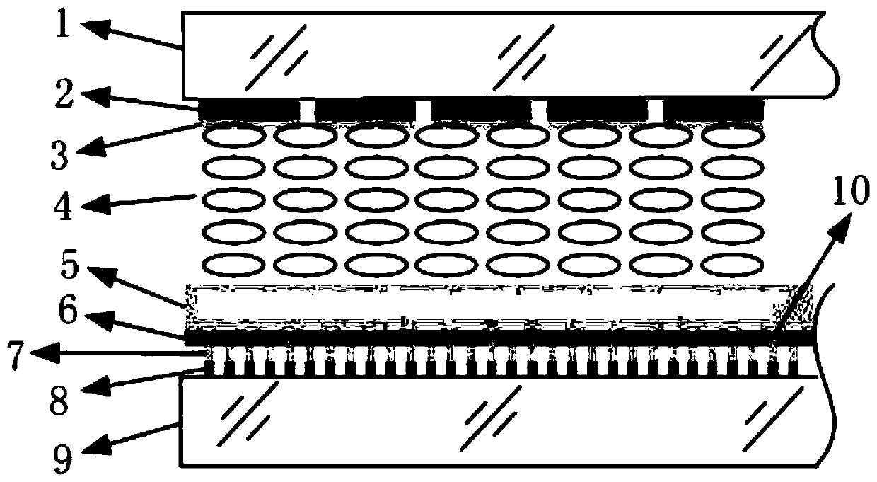
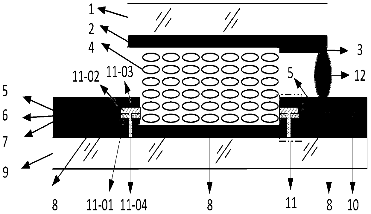
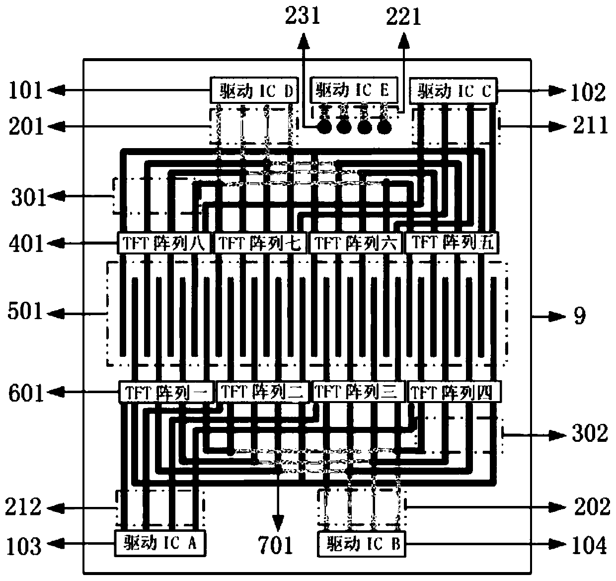
[0019] The invention provides a large-diameter liquid crystal optical phased array device, which mainly includes the via hole design of the film layer, the layout design of the liquid crystal peripheral wires, the design of the liquid crystal drive electrode, the design of the film layer of the upper substrate, the design of the film layer and size of the lower substrate, and the TFT array. and drive scheme design. The technical design of the film layer via means that an insulating layer is sandwiched between the two metal conductive layers of the upper substrate, and the metal wires of one layer and the metal wires of the other layer are electrically connected through the conductive holes. The size of the conductive hole is generally about 0.1um.

[0020] In the layout design of the peripheral wires described above, after a certain area is defined for the liquid crystal electrodes, there is no cross connection between the electrodes between two areas by wiring through via hol...


PUM


Abstract

The invention discloses a large-diameter liquid crystal optical phased array device, which comprises a first substrate, a liquid crystal molecular layer and a second substrate sequentially stacked from top to bottom; the first substrate sequentially includes a first substrate glass and a The first ITO electrode layer, the second substrate includes the second ITO electrode layer and the second substrate glass from top to bottom; the liquid crystal molecular layer is located between the first ITO electrode layer and the second ITO electrode layer; the second ITO electrode layer and the second ITO electrode layer There are multiple TFT arrays between the second metal conductive layers. The present invention selects the ITO film layer in the liquid crystal working area, and adopts a layer of ITO conductive layer and two metal conductive layers in the wiring layer of the non-liquid crystal working area. An insulating layer is plated between the conductive layers for electrical isolation, and two layers of metal Part of the electrodes on the conductive layer are designed with via holes together with the process design. This design greatly reduces the wiring area around the liquid crystal, increases the integration and area utilization, improves the deflection accuracy, and solves the problem of liquid crystal optical phased array aperture. small problem.

Description

technical field [0001] The invention relates to a large-diameter liquid crystal optical phased array device, which belongs to the liquid crystal optoelectronic device technology. The liquid crystal optoelectronic device can be used in the fields of laser communication, laser weapons and laser radar based on the liquid crystal optical phased array. Background technique [0002] With the advancement of technology, liquid crystal optical phased array has been proved to be a new method to realize non-mechanical beam deflection and spatial light modulation. Compared with the traditional beam deflection method, the liquid crystal optical phased array has the advantages of small size, low power consumption, high precision, and agility. With the rapid development of lidar, high-power laser beam combining, space information relay and forwarding, and the construction of space laser communication networks, the requirements for the caliber of liquid crystal optical phased arrays are als...

Claims


Application Information

Patent Timeline
Patent Type & Authority Patents(China)
IPC IPC(8): G02F1/29G02F1/1362
CPCG02F1/136227G02F1/292
Inventor 汪相如卓儒盛贺晓娴周庄奇
Owner UNIV OF ELECTRONICS SCI & TECH OF CHINA
Learn More