Multi-wavelength GaN-based asymmetric quantum well surface emitting laser and manufacturing method thereof
A technology for emitting lasers and quantum wells, which is applied in the direction of lasers, phonon exciters, and laser components, etc., can solve the problems of lack of controllability of laser wavelengths, and achieve commercialization and practicality, low production costs, and threshold value low effect
- Summary
- Abstract
- Description
- Claims
- Application Information
AI Technical Summary
Problems solved by technology
Method used
Image
Examples
Embodiment 1
[0053] Embodiment 1: Design method of asymmetric quantum well active region.
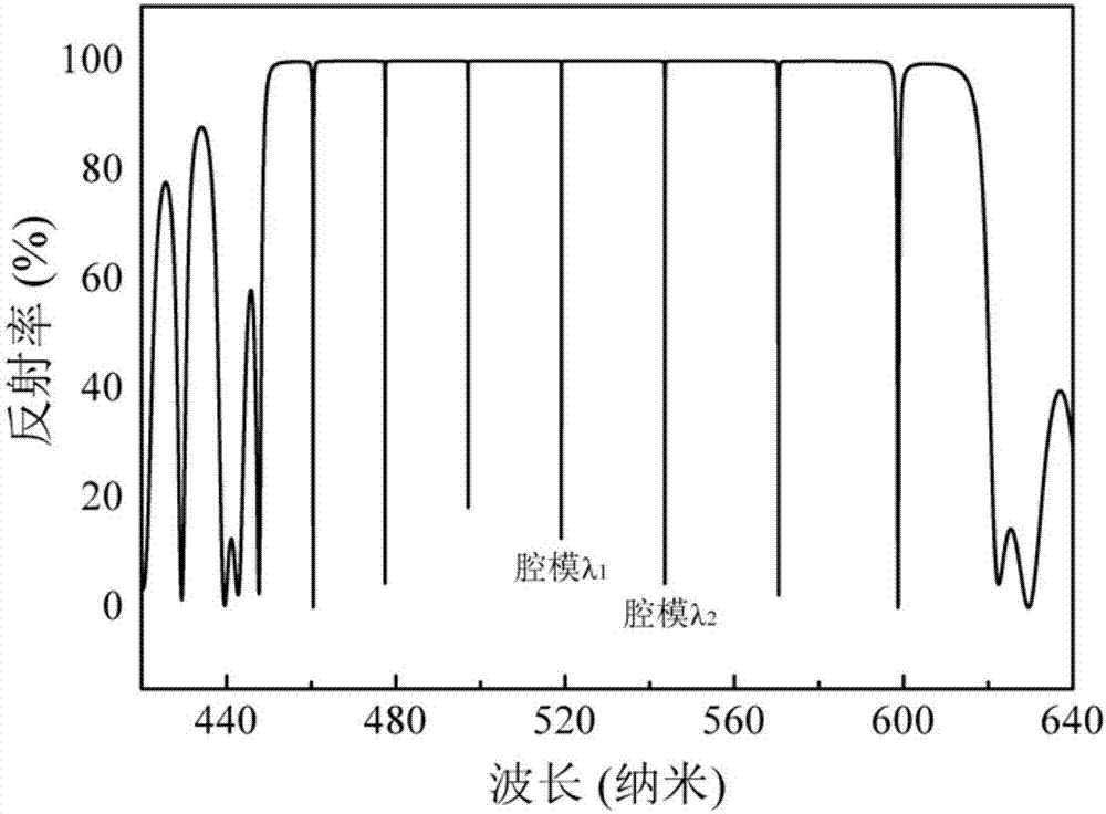
[0054] (1) For example, to prepare a laser with a wavelength of λ 1 and lambda 2 The dual-wavelength GaN-based asymmetric quantum well surface-emitting laser, then we can obtain the above two cavity modes (λ 1 , lambda 2 ) device structure, such as figure 1 shown. where the cavity mode λ 1 and the cavity mode λ 2 Corresponding to two wavelengths of 519 nanometers and 543 nanometers respectively, which are obtained under the condition that the laser cavity length is set to 2 microns, we can adjust the position of the cavity mode by changing the cavity length. Software such as TFCalc can be used for the simulation design of the cavity length and cavity mode of the laser.
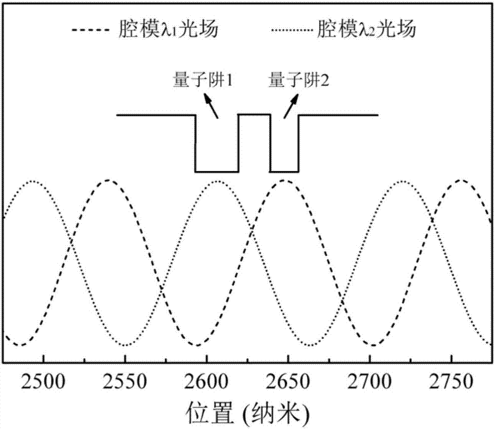
[0055] (2) Set the cavity length and cavity mode (λ 1 , lambda 2 ), the next step is to set the spatial position of the asymmetric quantum well in the resonant cavity. like figure 2 As shown, first use TFCalc software t...
Embodiment 2
[0057] Embodiment 2: Device preparation process flow.
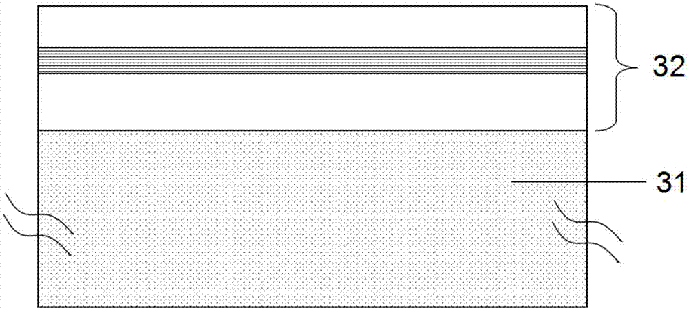
[0058] (1) if image 3 As shown, a GaN-based epitaxial wafer 32 with the asymmetric quantum well active region is grown on a sapphire substrate 31 by MOCVD, including a GaN low-temperature buffer layer (30 nanometers), an undoped GaN layer (2 micrometers) , Si-doped n-type GaN layer (2 microns), InGaN / GaN asymmetric quantum well active region (GaN barrier is 10 nanometers, InGaN wells are 2 nanometers and 5 nanometers respectively, a total of two groups), Mg-doped AlGaN layer (200nm) and Mg-doped p-type GaN layer (500nm), etc., and perform high-temperature annealing after the epitaxial wafer growth is completed to increase the hole concentration.
[0059] (2) if Figure 4 , performing photolithography on the GaN-based epitaxial wafer, and then using magnetron sputtering or electron beam evaporation to grow a distributed Bragg reflector, and then obtain a patterned distributed Bragg reflector 41 by a stripping method; th...
PUM
| Property | Measurement | Unit |
|---|---|---|
| Surface roughness | aaaaa | aaaaa |
Abstract
Description
Claims
Application Information


