Wafer-level back gold chip packaging structure and packaging method thereof

A technology of packaging structure and packaging method, which is applied to electrical components, electrical solid devices, circuits, etc., can solve the problems of scrapping and short-circuit failure of the packaging body, and achieve the effects of low power loss, material cost saving, and easy operation.

Active Publication Date: 2018-04-13
JIANGYIN CHANGDIAN ADVANCED PACKAGING CO LTD
View PDF6 Cites 8 Cited by
  • Summary
  • Abstract
  • Description
  • Claims
  • Application Information

AI Technical Summary

Problems solved by technology

During the welding process of the small package, its own weight is relatively light, and it is very easy to cause a short circuit failure due to the phenomenon of tin climbing during the welding process, or in the embedded high-density package, the entire package may be damaged due to displacement and contact with other chips. The package is scrapped

Method used


Image

  • Wafer-level back gold chip packaging structure and packaging method thereof
  • Wafer-level back gold chip packaging structure and packaging method thereof
  • Wafer-level back gold chip packaging structure and packaging method thereof

Examples


Embodiment

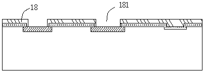
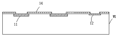
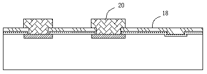
[0055] A packaging structure of a gold-backed chip of the present invention, such as figure 1 shown. The front side of the silicon base body 10 is provided with several chip electrodes 11 and functional sensing areas (not shown), the chip insulating layer 14 covers the silicon base body 10 and exposes the chip electrodes 11, and the chip insulating layer 14 covers the silicon base body The remainder of the scribe lane 12 of 10. The chip insulating layer 14 covers the remaining part of the scribe line 12 of the silicon base body 10 and extends outward to form a chip insulating layer extension 141 . The front protective layer 18 covers the chip insulation layer 14 and opens the front protective layer opening 181 to expose the chip electrode 11 again. The upper surface of the chip electrode 11 is provided with a metal bump 20 exposing the front protective layer 18. The metal bump 20 is made of copper or tin. , tin-silver alloy or Ni / Au, Ni / Pd / Au and other composite structures. ...


PUM


Abstract

The present invention discloses a back gold chip packaging structure and a packaging method thereof, belonging to the technical field of semiconductor packaging. A plurality of chip electrodes and front protective layers are arranged at the front surface of a silicon-based body, each front protective layer is provided with one front protective layer opening to expose chip electrodes again, and metal bump are arranged at the surfaces of the chip electrodes. The back surface of the silicon-based body is provided with a back gold layer, the back gold layer is in bonding connection with the back surface of the silicon-based body through a back gold bonding layer. A plastic packaging layer packages exposed surfaces of the back gold layer and the silicon-based body, and a plastic packaging layeropening is arranged to expose the exposed surface of the back surface of the back gold layer. The wafer-level back gold chip packaging structure and the packaging method thereof are simple in packaging flow, the silicon face processing technology, the back gold technology, the plastic packaging material ablation and the de-bonding technology are completed on a wafer, and therefore, the wafer-level back gold chip packaging structure and the packaging method thereof accord with future development direction of semiconductor manufacturing.

Description

technical field [0001] The invention relates to a packaging structure and a packaging method for a wafer-level gold-backed chip, belonging to the technical field of semiconductor packaging. Background technique [0002] In recent years, Embedded Package has received more and more attention from the industry. Embedded packages often have better thermal management and reliability advantages than other package structures. In this package, the backside of the chip is usually ground and metallized to reduce power loss or improve the heat dissipation performance of the power chip, and is embedded in an IC substrate for final packaging. [0003] In the embedded packaging structure, the metal layer on the back is used as a pole of the device, and usually requires a process that can withstand laser ablation, which puts forward higher requirements for the thickness of the back gold. [0004] At this stage, most of the chip back gold processes use precious metal structures, including...

Claims


Application Information

Patent Timeline
Patent Type & Authority Applications(China)
IPC IPC(8): H01L23/31H01L23/492H01L21/56H01L21/683
CPCH01L21/56H01L21/6835H01L23/3185H01L23/4924H01L2221/68345
Inventor 陈海杰陈栋胡正勋孙超张黎陈锦辉赖志明
Owner JIANGYIN CHANGDIAN ADVANCED PACKAGING CO LTD
Why Eureka
Try Eureka