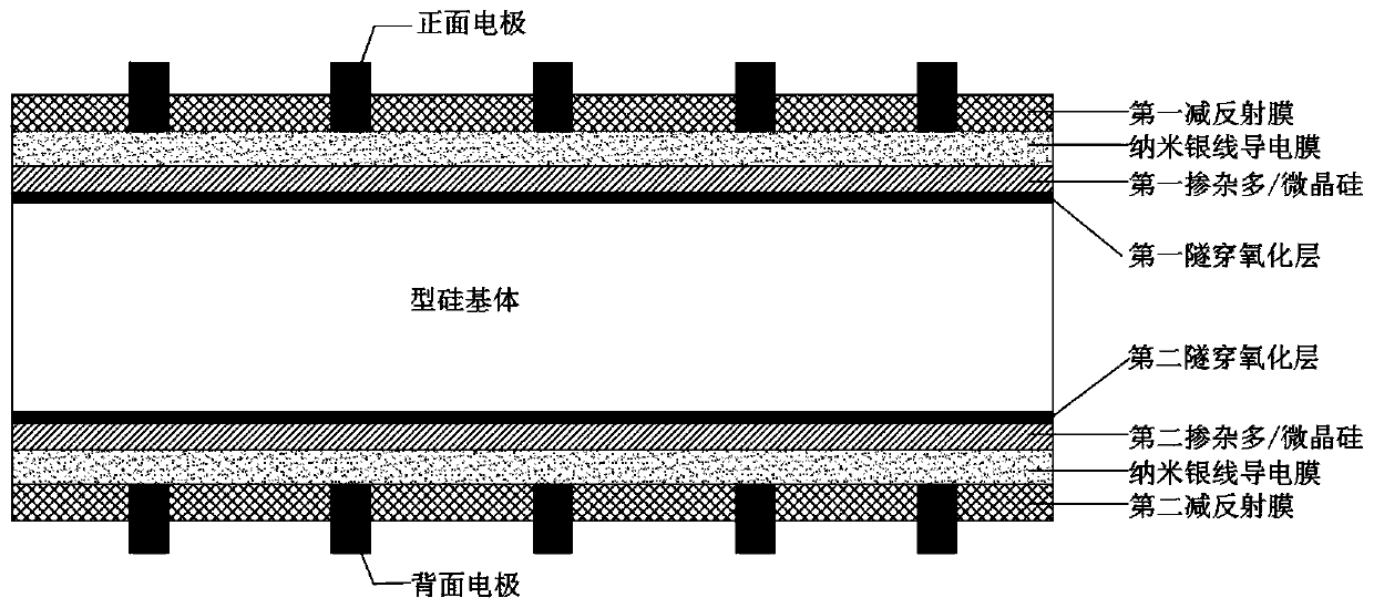
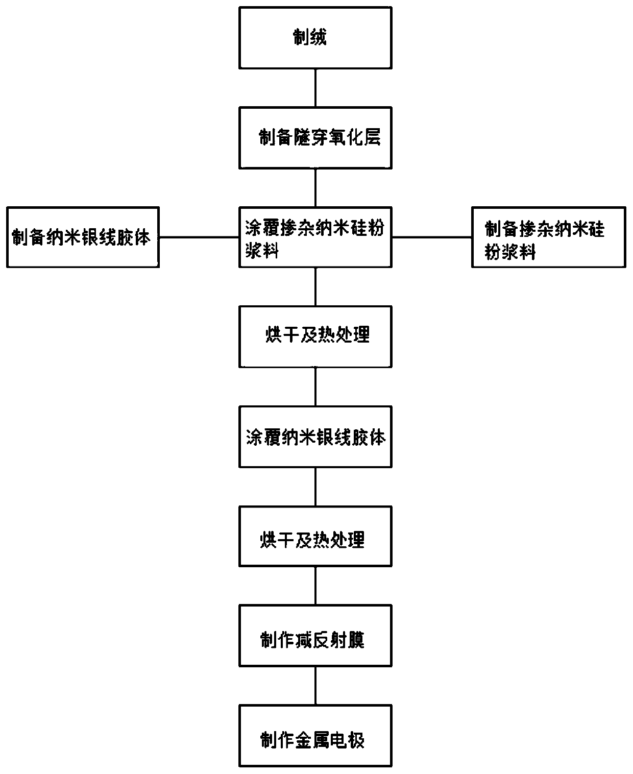
A kind of manufacturing method of passivated contact solar cell
A technology of a solar cell and a manufacturing method, applied in the field of solar cells, can solve the problems of reduction, high process control and environmental requirements, difficult manufacturing cost of a transparent conductive film, etc., achieves simple process, advantages of light transmittance and electrical conductivity, and reduces light The effect of occlusion area
- Summary
- Abstract
- Description
- Claims
- Application Information
AI Technical Summary
Problems solved by technology
Method used
Image
Examples
Embodiment 1
[0038] A method for making a passivated contact solar cell, comprising the following steps:
[0039] Step 1: Texture the P-type monocrystalline silicon wafer in NaOH hot solution, and wash to remove the dirt and damaged layer on the surface of the silicon wafer, and form a pyramidal light-trapping structure on the surface.
[0040] Step 2: Place the textured silicon wafer in ozone water with an ozone concentration of 50 ppm for 15 minutes to form a 1.2nm dense silicon oxide film on the surface of the silicon wafer.
[0041] Step 3: Prepare doped nano silicon powder slurry and nano silver wire colloid respectively.
[0042] The slurry doped with nano-silicon powder includes: ① Nano-crystalline silicon powder, with a mass fraction of 30% and a particle size of about 100nm. ②A slurry doped with nano-silicon powder is doped with boric acid, and the mass fraction of boron is 10^-7; another slurry doped with nano-silicon powder is doped with phosphoric acid, and the mass fraction o...
Embodiment 2
[0051] Step 1: forming an inverted pyramid structure on the surface of the N-type single crystal silicon wafer by catalytic chemical etching with nanometer metal particles.
[0052] Step 2: Place the textured silicon wafer in a thermal oxidation furnace in an oxygen atmosphere at 800° C. for 10 minutes to form a 2nm dense silicon oxide film on the surface.
[0053] Step 3: Prepare doped nano silicon powder slurry and nano silver wire colloid respectively.
[0054] The slurry doped with nano-silicon powder includes: ① Nano-crystalline silicon powder, with a mass fraction of 70% and a particle size of about 300nm. ② One kind of doped nano-silicon powder slurry is doped with boric acid, and the mass fraction of boron element is 10^-5; the other doped nano-silicon powder slurry is doped with phosphoric acid, and the mass fraction of phosphorus element is 10 ^-5. ③ According to the performance of the slurry, add the organic additive terpineol in proportion.
[0055] The nano sil...
PUM
| Property | Measurement | Unit |
|---|---|---|
| thickness | aaaaa | aaaaa |
| thickness | aaaaa | aaaaa |
| particle diameter | aaaaa | aaaaa |
Abstract
Description
Claims
Application Information
 - R&D
- Intellectual Property
- Life Sciences
- Materials
- Tech Scout
- Unparalleled Data Quality
- Higher Quality Content
- 60% Fewer Hallucinations
Browse by: Latest US Patents, China's latest patents, Technical Efficacy Thesaurus, Application Domain, Technology Topic, Popular Technical Reports.
© 2025 PatSnap. All rights reserved.Legal|Privacy policy|Modern Slavery Act Transparency Statement|Sitemap|About US| Contact US: help@patsnap.com


