Method for preparing grooved anode Schottky diode

A technology of Schottky diodes and anodes, which is applied in semiconductor/solid-state device manufacturing, electrical components, circuits, etc., and can solve problems such as reducing turn-on voltage and reverse leakage current

Inactive Publication Date: 2018-05-29
INST OF SEMICONDUCTORS - CHINESE ACAD OF SCI
View PDF3 Cites 0 Cited by
  • Summary
  • Abstract
  • Description
  • Claims
  • Application Information

AI Technical Summary

Problems solved by technology

Therefore, it is difficult to simply change the barrier height of the Schottky contact while reducing the turn-on voltage and reverse leakage current

Method used


Image

  • Method for preparing grooved anode Schottky diode
  • Method for preparing grooved anode Schottky diode
  • Method for preparing grooved anode Schottky diode

Examples


preparation example Construction

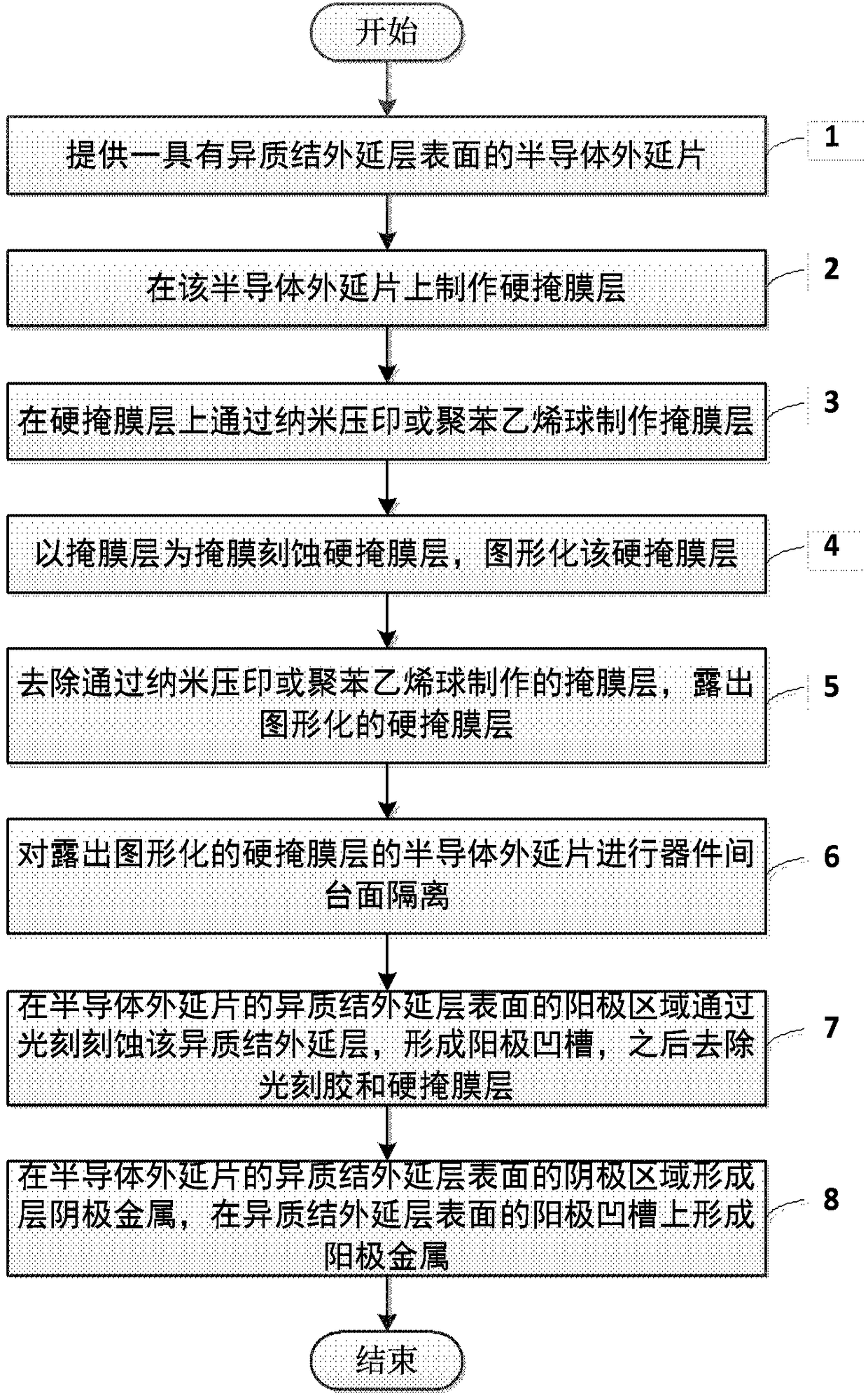
[0010] Such as figure 1 As shown, the preparation method of the recessed anode Schottky diode provided by the present invention comprises the following steps:

[0011] Step 1: Provide a semiconductor epitaxial wafer with a heterojunction epitaxial layer surface; the semiconductor epitaxial wafer can be a gallium nitride-based heterojunction epitaxial wafer, a gallium arsenide-based heterojunction epitaxial wafer, or silicon carbide with lateral conductivity epitaxial wafers, but not limited thereto.

[0012] Step 2: making a hard mask layer on the semiconductor epitaxial wafer; the hard mask layer is a material having an etching ratio with the semiconductor epitaxial wafer, including materials such as silicon dioxide, silicon nitride, nickel or gold.

[0013] Step 3: Make a mask layer by nanoimprinting or polystyrene spheres on the hard mask layer; the mask layer made by nanoimprinting or polystyrene spheres on the hard mask layer is made of nanoimprint Compared with the nan...

Embodiment 1

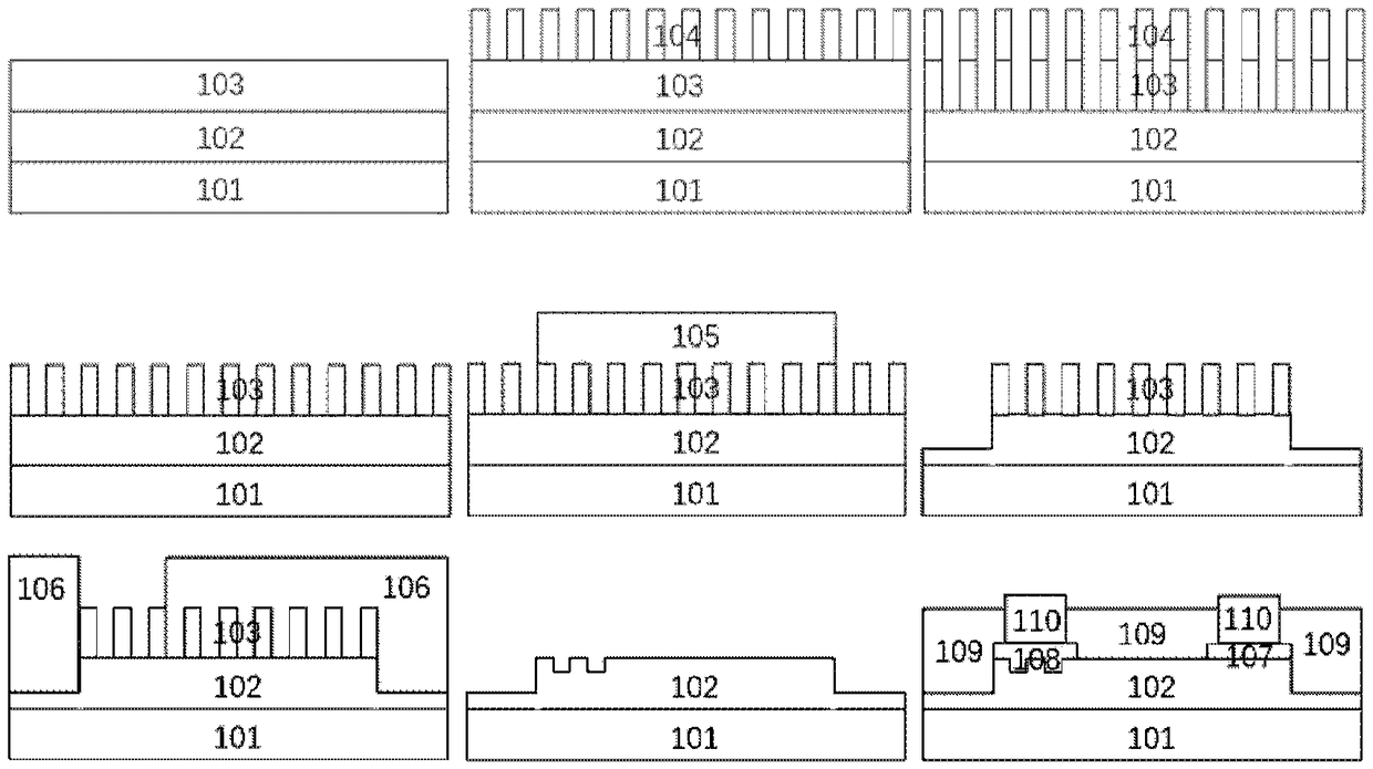
[0022] figure 2 It is a flow chart of the preparation process of an AlGaN / GaN heterojunction recessed anode Schottky diode using a sapphire substrate according to an embodiment of the present invention. The method includes the following steps:

[0023] Step 21: providing an epitaxial wafer, the epitaxial wafer is grown on the substrate 101 of sapphire material, and the AlGaN / GaN heterojunction epitaxial layer 102 is grown by MOCVD;

[0024] Step 22: On the epitaxial wafer, use PECVD equipment to deposit SiO 2 as a hard mask layer 103;

[0025] Step 23: On the hard mask layer 103, make a mask layer 104 by nanoimprinting technology;

[0026] Step 24: Using the mask layer 104 as a mask, use ICP equipment to etch the SiO in the hard mask layer 103 2 , to pattern the hard mask layer 103;

[0027] Step 25: using sulfuric acid hydrogen peroxide to remove the mask layer 104;

[0028] Step 26: Spread the glue and expose on the patterned hard mask layer 103 to form a mesa mask 105...

Embodiment 2

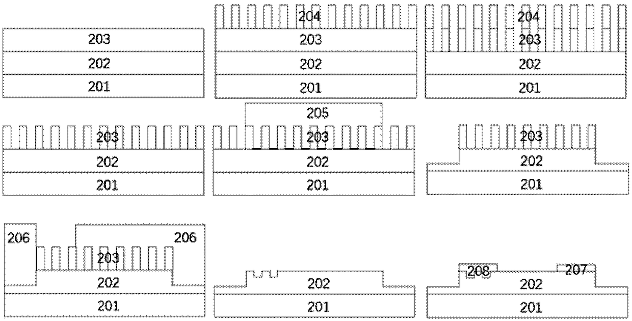
[0033] image 3 It is a flow chart of the preparation process of an InAlN / GaN heterojunction recessed anode Schottky diode using a silicon substrate according to an embodiment of the present invention. The method includes the following steps:

[0034] Step 31: providing an epitaxial wafer, the epitaxial wafer is grown on the substrate 201 of silicon material, and the InAlN / GaN heterojunction epitaxial layer 202 is grown by MOCVD;

[0035] Step 32: on the epitaxial wafer, use PECVD equipment to deposit SiNx as the hard mask layer 203;

[0036] Step 33: Fabricate a mask layer 204 on the hard mask layer 203 by nanoimprinting technology;

[0037] Step 34: Using the mask layer 204 as a mask, use ICP equipment to etch the SiNx in the hard mask layer 203 to pattern the hard mask layer 203;

[0038] Step 35: using sulfuric acid hydrogen peroxide to remove the mask layer 204;

[0039] Step 36: Spread the glue and expose on the patterned hard mask layer 203 to form a mesa mask 205, and...


PUM

PropertyMeasurementUnit
Thicknessaaaaaaaaaa

Abstract

The invention discloses a method for preparing a grooved anode Schottky diode. The method comprises the steps of: providing a semiconductor epitaxial wafer; manufacturing a hard mask layer on the semiconductor epitaxial wafer; manufacturing a mask layer on the hard mask layer; and using the mask layer as a mask for etching the hard mask layer, and patterning the hard mask layer; removing the masklayer to expose the patterned hard mask layer; performing inter-device mesa isolation on the semiconductor epitaxial wafer on which the patterned hard mask layer is exposed; etching a heterojunction epitaxial layer to form an anode groove in an anode region on the surface of the heterojunction epitaxial layer of the semiconductor epitaxial wafer, and then removing a photoresist and the hard mask layer; and forming a layer of cathode metal in a cathode region on the surface of the heterojunction epitaxial layer of the semiconductor epitaxial wafer. The method utilizes a nanoimprint technology or a polystyrene ball paving technology to realize the nanoscale anode groove, so as to prepare the Schottky diode having the good positive conducting features such as low turn-on voltage, low conducting resistance and high saturation current as well as good reverse turn-off features such as low electric leakage and high breakdown voltage simultaneously.

Description

technical field [0001] The invention belongs to the technical field of semiconductors, and in particular relates to a method for preparing a recessed anode Schottky diode, which can reduce conduction voltage drop, conduction resistance, reverse leakage current, and improve forward conduction current and reverse breakdown voltage. Background technique [0002] The barrier height of the Schottky diode is smaller than that of the PN junction, and its turn-on voltage and conduction voltage drop are smaller than those of the PN diode, which can reduce the power loss in the circuit. In addition, Schottky diodes have no minority carrier storage effect, short reverse recovery time, and fast switching speed. At the same time, due to the low junction capacitance, Schottky diodes can adapt to high frequency applications. The turn-on voltage and reverse leakage current of the Schottky diode are mainly determined by the Schottky contact. The barrier height of the Schottky contact is sm...

Claims


Application Information

Patent Timeline
IPC IPC(8): H01L21/329H01L29/872
CPCH01L29/6606H01L29/66143H01L29/872
Inventor 程哲张连张韵
Owner INST OF SEMICONDUCTORS - CHINESE ACAD OF SCI
Why Eureka
Try Eureka