an organic light emitting diode

A light-emitting diode, an organic technology, applied in the direction of organic semiconductor devices, electric solid-state devices, semiconductor devices, etc., can solve the problems of low luminous efficiency of organic light-emitting diodes, achieve the effect of short life and improve luminous efficiency

Active Publication Date: 2019-12-03
KUNSHAN GO VISIONOX OPTO ELECTRONICS CO LTD +1
View PDF8 Cites 0 Cited by
  • Summary
  • Abstract
  • Description
  • Claims
  • Application Information

AI Technical Summary

Problems solved by technology

[0009] The embodiment of the present application provides an organic light emitting diode, which is used to solve the problem that the light emitting efficiency of the organic light emitting diode is low due to the use of existing light emitting materials as the host material of the light emitting layer of the organic light emitting diode

Method used


Image

  • an organic light emitting diode
  • an organic light emitting diode
  • an organic light emitting diode

Examples


preparation example Construction

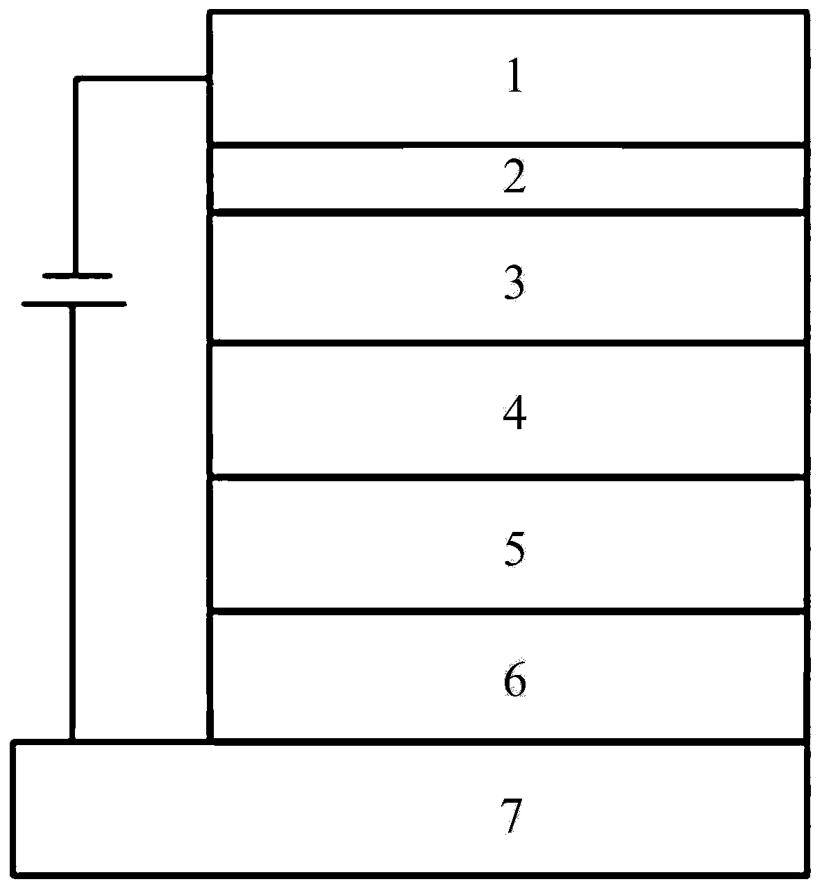
[0049] The present invention also provides a method for preparing the organic light-emitting diode, comprising sequentially depositing a hole injection layer 6, a hole transport layer 5, a light-emitting layer 4, an electron transport layer 3, an electron injection layer 2 and a cathode 1 stacked on an ITO substrate. , and then encapsulate.

[0050]The substrate can be glass or a flexible substrate, and the flexible substrate can be made of polyester, polyimide compound material or thin metal sheet. The lamination and packaging can adopt any suitable method known to those skilled in the art.

Embodiment 1

[0076] In this comparative example, ITO (indium tin oxide) is used as the anode; NPB is used as the hole injection layer; TCTA is used as the hole transport layer; The mass percentage of doping in is 3wt%); Bphen is used as the electron transport layer; Li(5nm) / Al is used as the cathode. The structure is as follows:

[0077] ITO / NPB(40nm) / TCTA(10nm) / CBP: 1wt%;

[0078] Ir(bt)2(acac)(30nm) / Bphen(40nm) / LiF(5nm) / Al.

Embodiment 2

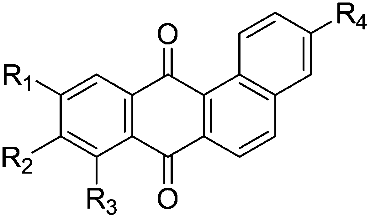
[0080] The structure of this example is the same as that of Comparative Example 1 except that the host material used in the light-emitting layer 4 is the compound of formula (2-6) of the present invention. The structure is as follows:

[0081] ITO / NPB(40nm) / TCTA(10nm) / Formula (1-9): 1 wt% Ir(bt)2(acac)(30nm) / Bphen(40nm) / LiF(5nm) / Al.

[0082] Table 2

[0083]

[0084] The red phosphorescent organic electroluminescent device of the present invention uses a new heat-activated sensitized fluorescent material as the main body sensitized phosphorescent material device, and the current of the heat-activated sensitized fluorescent material sensitized phosphorescent material device is higher than that of the common main body sensitized phosphorescent material and the reported thermally activated sensitized fluorescent material sensitized phosphorescent material device. The efficiency is high, and the voltage is the lowest, indicating that the ΔEST of the heat-activated sensitized f...


PUM


Abstract

The application discloses an organic light emitting diode, which is used to solve the problem of low luminous efficiency of the organic light emitting diode caused by using the existing light emitting material as the host material of the light emitting layer of the organic light emitting diode. The organic light emitting diode includes a light-emitting layer, the host material of the light-emitting layer includes a TADF material, the host material is doped with a phosphorescent material, and the TADF material has a general structural formula shown in the following formula (I): wherein, R 1 , R 2 , R 3 and R 4 Independently selected from the electron donor group, the electron donor group is phenoxazinyl, phenothiazinyl, 9,9-dimethylacridinyl, 9-methylphenazinyl, 9-phenyl Phenazinyl, 4-phenoxazinyl-1-phenyl, 4-phenothiazinyl-1-phenyl, 4-(9,9-dimethyl)acridinyl-1-phenyl, 4- (9-methyl)phenazinyl-1-phenyl, 4-(9-phenyl)phenazinyl-1-phenyl, 3,5-dicarbazolyl-1-phenyl, 4-diphenylamine One or more of the base-1-phenyl groups.

Description

technical field [0001] The present application relates to the field of organic light emitting display technology, and in particular to an organic light emitting diode. Background technique [0002] Organic Light-Emitting Diode (OLED) is a current-driven light-emitting device that uses organic materials as active materials. Specifically, organic semiconductor materials and organic light-emitting materials are driven by an electric field through carrier injection and Composite technology that leads to luminescence. Unlike inorganic materials, organic materials have the characteristics of low synthesis cost, adjustable function, flexibility, and good film-forming properties. Moreover, devices based on organic materials are generally simple in manufacturing process, easy to prepare in large areas, environmentally friendly, and can adopt thin film preparation methods with low operating temperature, so they have the advantage of low manufacturing cost and have great application p...

Claims


Application Information

Patent Timeline
Patent Type & Authority Patents(China)
IPC IPC(8): H01L51/50H01L51/54
CPCH10K85/60H10K50/12H10K2101/27
Inventor 段炼张云阁刘嵩赵菲
Owner KUNSHAN GO VISIONOX OPTO ELECTRONICS CO LTD
Why Eureka
Try Eureka