Silicon carbide groove-shaped metal-oxide-semiconductor field-effect transistors (MOSFETs) and fabrication method thereof

A silicon carbide trench and silicon carbide substrate technology, which is applied in semiconductor/solid-state device manufacturing, electrical components, circuits, etc., can solve problems such as unfavorable long-term stable operation of devices, reduced gate dielectric reliability, and reduced device conduction characteristics. , to reduce the reliability of blocking work, improve the carrier mobility, and reduce the overlap area.

Active Publication Date: 2018-08-17
INST OF SEMICONDUCTORS - CHINESE ACAD OF SCI
View PDF5 Cites 6 Cited by
  • Summary
  • Abstract
  • Description
  • Claims
  • Application Information

AI Technical Summary

Problems solved by technology

[0003] However, on the one hand, the channel carrier mobility of silicon carbide trench MOSFET is still much lower than that of silicon carbide bulk material, thus reducing the conduction characteristics of the device; on the other hand, due to the critical breakdown electric field of silicon carbide Larger, the electric field in the gate dielectric rises sharply, especially the two-dimensional electric field concentration phenomenon at the groove corner is more serious, which makes the reliability of the gate dielectric of the SiC MOSFET working at high frequency, high temperature and high power greatly improved. reduced, thus detrimental to the long-term stability of the device

Method used


Image

  • Silicon carbide groove-shaped metal-oxide-semiconductor field-effect transistors (MOSFETs) and fabrication method thereof
  • Silicon carbide groove-shaped metal-oxide-semiconductor field-effect transistors (MOSFETs) and fabrication method thereof
  • Silicon carbide groove-shaped metal-oxide-semiconductor field-effect transistors (MOSFETs) and fabrication method thereof

Examples


preparation example Construction

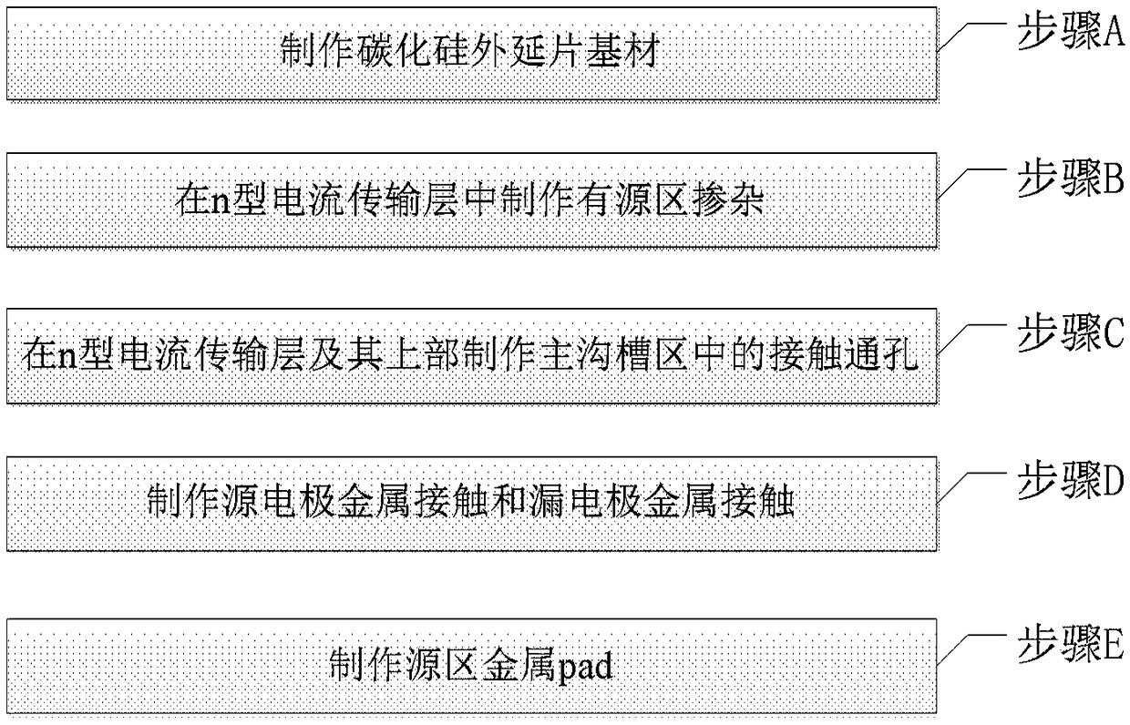
[0090] figure 2 It is a schematic diagram of the steps of the preparation method, such as figure 2 Shown, described preparation method comprises:

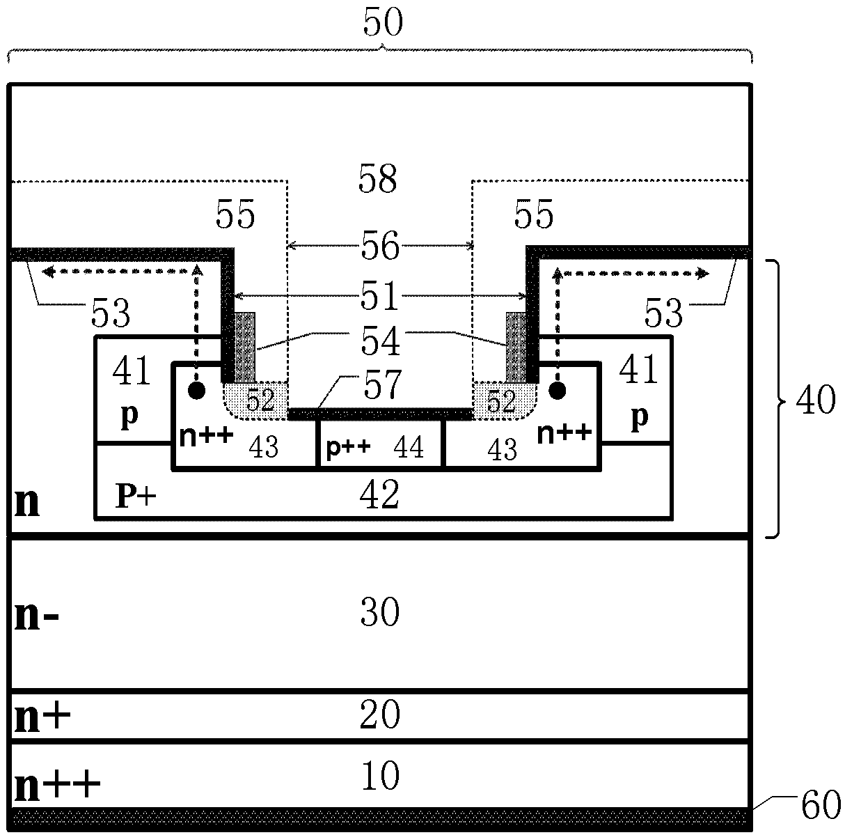
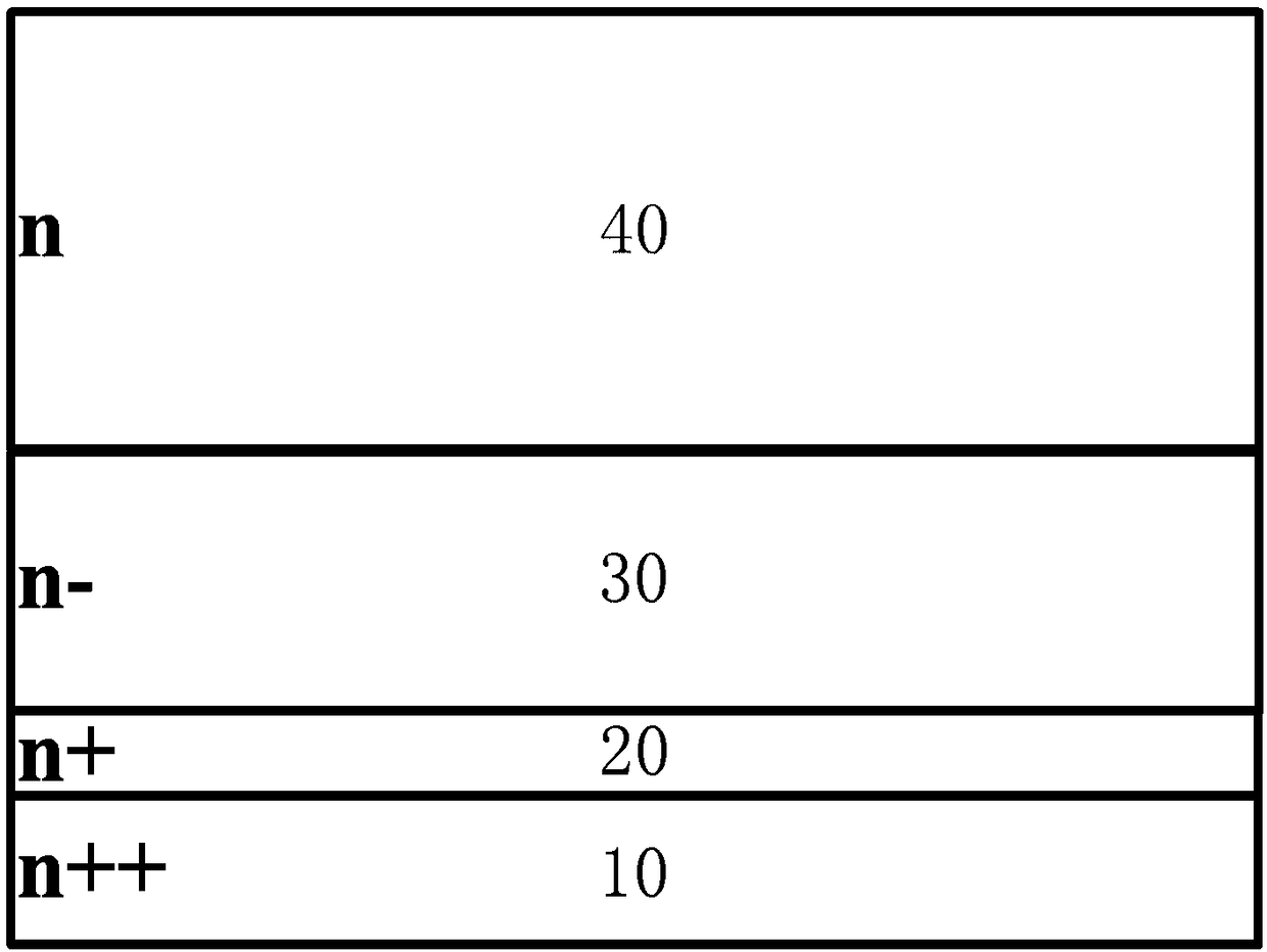
[0091] Step A: making a silicon carbide epitaxial substrate; including, epitaxially growing an n+ type buffer layer 20, an n-drift layer 30, and an n-type current transport layer 40 on the n++ type silicon carbide substrate 10 from bottom to top;

[0092] Step B: Doping the active region in the n-type current transport layer 40, including:

[0093]Sub-step B1: Deposit an implantation mask on the n-type current transport layer 40, pattern it by photolithography, and use doping methods such as ion implantation to form a top-down p-type trench in the n-type current transport layer 40 Road layer 41 and p+ type shielding layer 42;

[0094] In the sub-step B1, the doping concentration range of the p-type channel layer 41 is 1×10 16 cm -3 ~1×10 18 cm -3 , the distance between the upper surface and the upper surface of the n-type ...


PUM

PropertyMeasurementUnit
thicknessaaaaaaaaaa

Abstract

The invention provides silicon carbide groove-shaped metal-oxide-semiconductor field-effect transistors (MOSFETs) and a fabrication method thereof. Gate contact of the MOSFETs is arranged at a side wall of a main groove, source metal contact is formed at the bottom of the groove, electrons flow through an inversion layer at the side wall of the groove from bottom to top to form an inverse conduction channel different from traditional groove-shaped MOSFETs during positive conduction, a high electric field of a body region of a device is effectively shielded by the source metal contact at the bottom of the groove during reverse blocking, so that the gate dielectric field of the device is greatly reduced, and avalanche occurs at a PN junction of the body region of the device. The fabricated silicon carbide groove-shaped MOSFETs have relatively low positive conduction resistance and relatively high reverse blocking capability, and the static and dynamic working reliability of the device can be improved.

Description

technical field [0001] The invention relates to a silicon carbide trench type metal-oxide-semiconductor field effect transistor (MOSFET) structure and a preparation method thereof, in particular to a method for manufacturing silicon carbide trench type MOSFETs with a reverse conduction channel. Background technique [0002] Silicon carbide MOSFET is currently the fastest-growing wide-bandgap power semiconductor device. Compared with traditional silicon materials, silicon carbide has obvious advantages in physical and electrical properties, and plays an extremely important role in energy saving and emission reduction. Among them, MOSFET with vertical silicon carbide trench gate structure has a non-polar channel surface and has higher mobility and higher cell integration, making silicon carbide trench MOSFET a next-generation power electronic device It can be widely used in fields such as electric vehicles, charging piles, uninterruptible power supplies, and smart grids. [0...

Claims


Application Information

Patent Timeline
Patent Type & Authority Applications(China)
IPC IPC(8): H01L29/06H01L29/423H01L29/45H01L29/78H01L21/336H01L21/28
CPCH01L29/0684H01L29/401H01L29/4236H01L29/42364H01L29/45H01L29/66068H01L29/7827
Inventor 申占伟张峰赵万顺王雷温正欣闫果果刘兴昉孙国胜曾一平
Owner INST OF SEMICONDUCTORS - CHINESE ACAD OF SCI
Why Eureka
Try Eureka