A laser direct machining method for microwave substrate cavity

A processing molding and laser direct technology, applied in the direction of laser welding equipment, metal processing equipment, manufacturing tools, etc., can solve the problems of corrosion taper, low corrosion rate and cavity size consistency, etc., to achieve good compatibility, high control precision, good verticality

Active Publication Date: 2020-01-03
CHINA ELECTRONIC TECH GRP CORP NO 38 RES INST
View PDF7 Cites 0 Cited by
  • Summary
  • Abstract
  • Description
  • Claims
  • Application Information

AI Technical Summary

Problems solved by technology

[0004] Aiming at the problems of corrosion taper, low corrosion rate, and uniform size of the cavity in the cavity structure formed by the microwave substrate, the present invention provides a laser direct processing method for the cavity of the microwave substrate

Method used


Image

  • A laser direct machining method for microwave substrate cavity
  • A laser direct machining method for microwave substrate cavity
  • A laser direct machining method for microwave substrate cavity

Examples


Embodiment 1

[0041] Take the machining of a cavity with a plane size of 2 mm×2 mm and a depth of 100 μm on a substrate 1 of silicon material with a thickness of 0.4 mm and a thickness of 6 inches as an example.

[0042] The specific processing steps are as follows:

[0043] (1) Pretreatment of 6-inch substrate and protection of circuit graphics

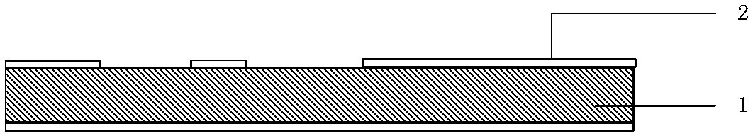
[0044] (1.1) Clean the substrate 1;

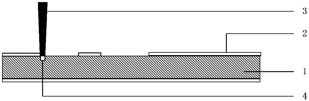
[0045] (1.2) see figure 1 and figure 2 1. Coat the surface of the cleaned substrate 1 with photoresist 2 to protect the surface circuit pattern. The thickness of the photoresist 2 is 5-10 μm, and open a window at the processing position of the cavity through photolithography and development.

[0046] (2) The laser beam etches the substrate to form a cavity

[0047] (2.1) see Figure 3-5 , at the opening position on the substrate 1, laser etching forms more than one cavity 7 on the substrate 1, and the angle between the cavity wall of the cavity 7 and the vertical direction is less than 5 degrees;

[004...

Embodiment 2

[0053] A stepped cavity with two steps is processed on a 6-inch silicon wafer with a thickness of 0.4 mm; in the stepped cavity, the large-sized cavity is located at the upper part, and the small-sized cavity is located at the lower part. The planar size of the large-size cavity is 2mm×2mm and the depth is 100μm, and the planar size of the small-size cavity is 1.5mm×1.5mm and the depth is 200μm.

[0054] The specific processing steps are as follows:

[0055] Step 1: Pre-treatment of silicon substrate and protection of circuit pattern; coat the surface of the cleaned silicon substrate with photoresist for surface circuit pattern protection, the thickness of photoresist is 5-10 μm, and pass photolithography and development in the cavity The body processing position opens the window.

[0056] Step 2: The laser beam etches the silicon substrate to form an upper cavity; select a laser with a wavelength of 355nm and a spot size of 0.015mm, and laser marking is carried out sequentia...

Embodiment 3

[0060] On a 1.2mm thick LTCC substrate, a cavity with a plane size of 2mm×5mm and a depth of 200μm is taken as an example.

[0061] The specific operation steps of LTCC substrate cavity laser processing are as follows:

[0062] Step 1: LTCC substrate pre-processing and circuit pattern protection

[0063] see figure 1 and figure 2 , Coat the surface of the cleaned LTCC substrate with photoresist to protect the surface circuit pattern, the thickness of the photoresist is 5-10 μm, and open a window at the cavity processing position through photolithography and development.

[0064] Step 2: Laser beam etching LTCC substrate to form a cavity

[0065] see Figure 3-5 , choose a laser with a wavelength of 355nm and a spot size of 0.015mm, and the laser marking is carried out in the order of crossing the number of processing passes in the horizontal and vertical directions. Laser processing parameters: laser energy 4.5W, laser spot overlap rate 75%, laser frequency 32KHz, markin...


PUM

PropertyMeasurementUnit
wavelengthaaaaaaaaaa
diameteraaaaaaaaaa
surface roughnessaaaaaaaaaa

Abstract

The invention provides a method for removing silicon-based material by adopting focused laser beams to form a cavity structure according to the purposes that a cavity structure formed microwave substrates is low in corrosion taper and corrosion speed and has cavity size consistency. The manufacturing method includes the steps that firstly, pre-treatment of the microwave substrates and circuit pattern protection are protected; secondly, laser beam etching is performed on the microwave substrates to form a cavity of a certain depth; and thirdly, microwave substrate after-treatment is performed.According to the method, grooves are formed in an etching manner due to moving of laser beams, and the grooves overlap with one another so that material removing of a certain area can be achieved. Repeated processing is performed in an area needing etching so that a certain etching depth can be achieved, and therefore the cavity structure of a certain depth can be formed. Laser energy is further utilized to clean the bottom of the cavity, and the purpose of cleanness is achieved while a base body is not damaged. The method has the beneficial effects that the control precision is high, efficiency is high, environment friendliness is achieved, the cavity wall perpendicularity is good, and compatibility with the microwave substrate circuit manufacturing process is good.

Description

technical field [0001] The invention belongs to the technical field of laser processing, and in particular relates to a laser processing method of an electronic circuit substrate, in particular to a microwave substrate cavity laser processing method. Background technique [0002] In multi-chip modules, commonly used circuit substrates such as alumina, LTCC, PCB, and silicon are not only used as mechanical support carriers for electronic components, but also provide electrical interconnection of circuits and channels for heat dissipation of circuits. With the development requirements of high integration, high frequency and high power of multi-chip components, it is an important development direction to form cavity structures on electronic substrates. The prepared cavity structure can be used to install chips in an embedded manner, which can increase the assembly density while shortening the interconnection lines between layers, reduce the influence of microwave discontinuity,...

Claims


Application Information

Patent Timeline
Patent Type & Authority Patents(China)
IPC IPC(8): B23K26/362B23K26/18B81C1/00
CPCB23K26/18B23K26/361B81B2203/0315B81C1/005
Inventor 王运龙王强文邱颖霞郭育华宋夏
Owner CHINA ELECTRONIC TECH GRP CORP NO 38 RES INST
Why Eureka
Try Eureka