High-reliability IGBT module packaging structure and processing technology

A packaging structure and reliability technology, applied in semiconductor/solid-state device parts, semiconductor devices, electrical components, etc., can solve the problems of chip size reduction and chip power density increase, so as to strengthen the bonding force and improve the overall thermal conductivity , The effect of excellent thermal conductivity

Active Publication Date: 2018-08-28
HUANGSHAN UNIV
View PDF7 Cites 8 Cited by
  • Summary
  • Abstract
  • Description
  • Claims
  • Application Information

AI Technical Summary

Problems solved by technology

With the increase of operating voltage and current of IGBT power semiconductor devices, and the continuous reduction of chip size, the power density of the chip increases sharply, which poses a great challenge to the reliability of its packaging.

Method used


Image

  • High-reliability IGBT module packaging structure and processing technology
  • High-reliability IGBT module packaging structure and processing technology
  • High-reliability IGBT module packaging structure and processing technology

Examples


Embodiment Construction

[0035] The present invention will be further described below in conjunction with drawings and embodiments.

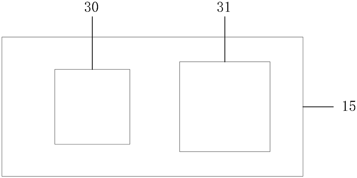
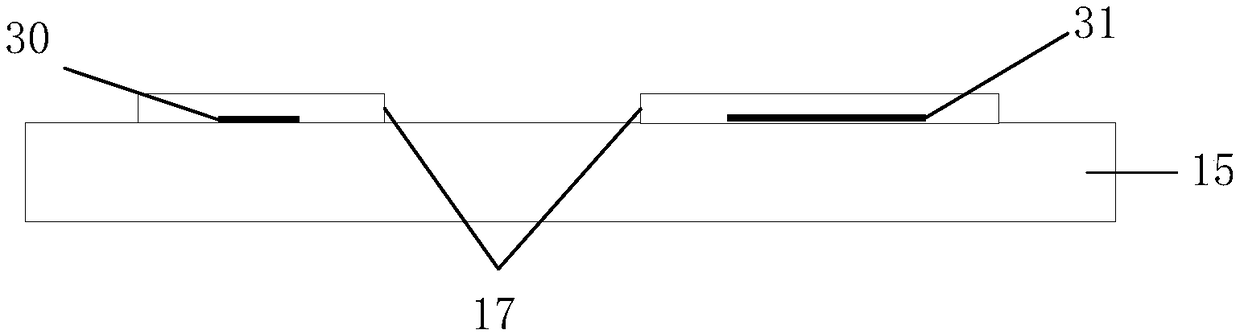
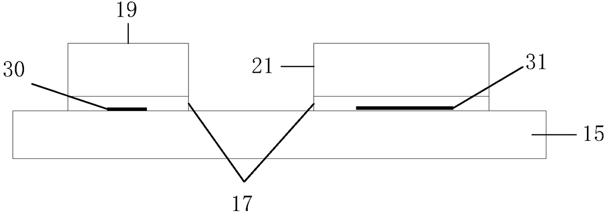
[0036] The present invention proposes a high-reliability IGBT module packaging structure, which generally includes: a DBC (direct copper clad) substrate with patterned growth of 2D-hBN on the upper surface, an IGBT chip, a FRD (fast recovery diode) chip, a bottom plate, and a solder layer , bonding wires, bus bars, plastic housings, and 2D-hBN filled reinforced potting silicone.

[0037] see figure 1 , in order to pattern-grow the first 2D-hBN thin film 30 on the central position of the connection area corresponding to the cathode of the FRD chip 19 on the upper surface of the DBC substrate 14 by chemical vapor deposition, and to connect the corresponding collector of the IGBT chip 21 on the upper surface of the DBC substrate 14 A second 2D-hBN thin film 31 is patterned and grown on the central position of the region. The first 2D-hBN thin film 30 and the second 2D-hB...


PUM


Abstract

The invention relates to a high-reliability IGBT module packaging structure and a processing technology. The packaging structure comprises a direct copper-clad substrate, an IGBT chip, a quick recovery diode chip, a bottom plate, a soldering flux layer, a bonded lead, a bus, a plastic shell and two-dimensional layered hexagonal boron nitride filled enhanced encapsulated silica gel, wherein two-dimensional layered hexagonal boron nitride is grown on the upper surface of the direct copper-clad substrate in a graphic manner. A two-dimensional layered hexagonal boron nitride thin film is grown onthe upper surface of the direct copper-clad substrate in a graphic manner through a chemical vapor deposition method. By virtue of excellent in-plane thermal conduction performance, partial hot spot heat of the high-power IGBT module can be quickly and transversely dissipated, heat can be conducted outwardly through the direct copper-clad substrate, and the highest temperature of the module is lowered; and meanwhile, by adopting the two-dimensional layered hexagonal boron nitride filled enhanced encapsulated silica gel for encapsulating, the thermal conduction performance of the conventional silica gel is improved, and module reliability is improved effectively.

Description

technical field [0001] The invention belongs to the technical field of semiconductors, and in particular relates to a packaging structure and processing technology of a high-reliability IGBT module. Background technique [0002] Insulated gate bipolar transistor (IGBT) is a composite full-control voltage-driven power semiconductor device composed of metal oxide semiconductor field effect transistor (MOSFET) and bipolar transistor (BJT). It is easy to drive MOSFET and fast switching speed. The advantages of BJT and the advantages of small on-state voltage drop and large current carrying capacity have become the mainstream of power semiconductor devices. [0003] The application of IGBT is inseparable from packaging, which directly affects the electrical, thermal and mechanical properties of the device, as well as the reliability and cost of the device. In addition, packaging plays a decisive role in the miniaturization, high integration and multi-function of devices and even...

Claims


Application Information

Patent Timeline
Patent Type & Authority Applications(China)
IPC IPC(8): H01L25/07H01L23/373H01L23/29H01L21/50H01L21/56
CPCH01L25/072H01L21/50H01L21/56H01L23/291H01L23/373H01L2924/181H01L2224/48091H01L2224/48137H01L2224/48227H01L2924/00014H01L2924/00012
Inventor 鲍婕王哲刘琦占林松宁仁霞何聚许媛
Owner HUANGSHAN UNIV
Why Eureka
Try Eureka