

Organic electroluminescent device and preparation method thereof
An electroluminescent device, electroluminescent technology, applied in the direction of electric solid device, semiconductor/solid state device manufacturing, electrical components, etc., can solve the problems of ultra-high vacuum conditions, unsuitable for large-scale production, etc., to achieve high material utilization, suitable for The effect of large-scale production and a wide range of choices
- Summary
- Abstract
- Description
- Claims
- Application Information
AI Technical Summary
Problems solved by technology
Method used
Image

Examples
preparation example Construction
[0030] The method for preparing the above-mentioned organic electroluminescent device is characterized in that it comprises the following steps:
[0031] ①Use de-detergent, deionized water, acetone and ethanol solutions to ultrasonically clean the substrate with the anode layer in sequence, and put it in an oven for drying after cleaning.
[0032] ② On the anode layer, the hole injection layer, the hole transport layer, the light-emitting layer and the electron transport layer are sequentially prepared by a wet process method, and then moved into a vacuum coating chamber to prepare the cathode layer to obtain an organic electroluminescent device. Preferably, the hole injection layer, the hole transport layer, the light-emitting layer and the electron transport layer are sequentially prepared on the anode layer of the substrate through a wet process, and the wet process can take spin coating, dip coating, inkjet printing, roll coating , one or more of LB films. The cathode lay...
Embodiment 1
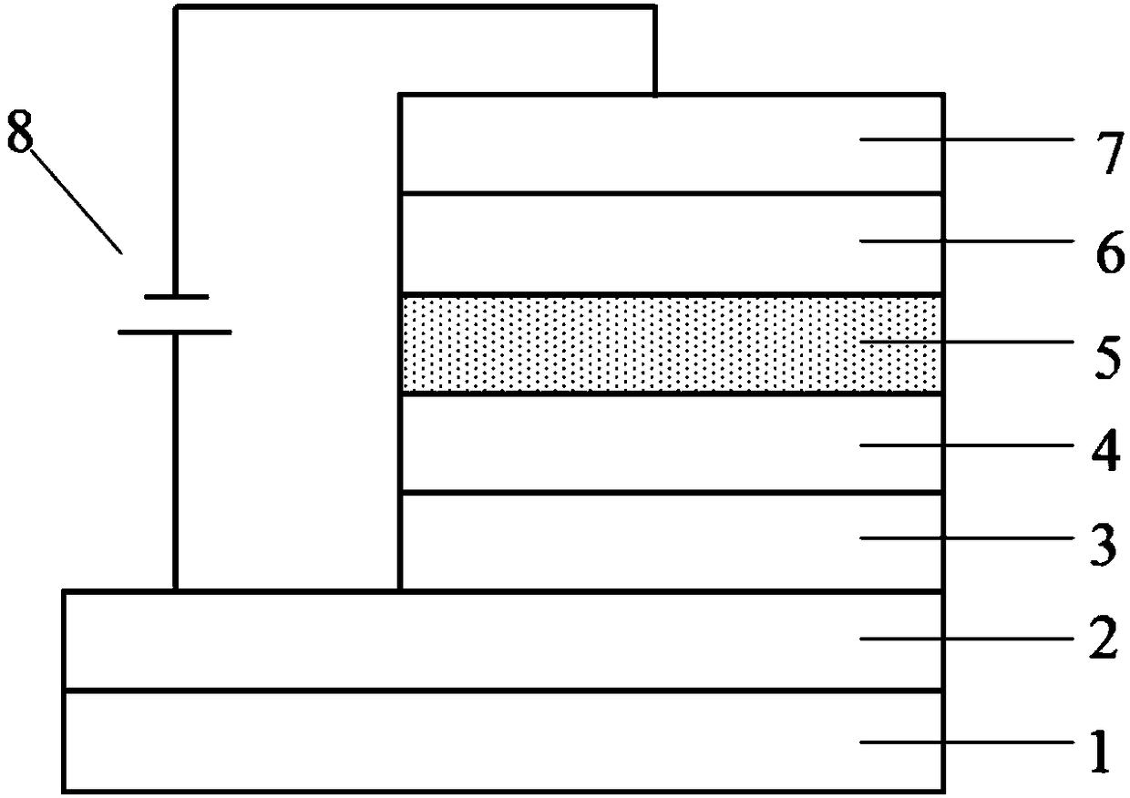
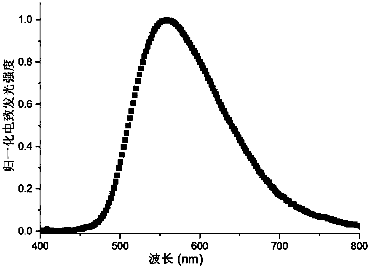
[0042] Such as figure 1 As shown, the hole injection layer 3 in the device structure is PEDOT:PSS, the hole transport layer 4 is TAPC, the host material in the yellow light emitting layer 5 is CBP, and the guest material is a yellow light emitting material emitterY with thermally activated delayed fluorescence characteristics, Its electron donor is a phenothiazine group, the electron acceptor is a benzophenone group, and the doping mass ratio is a guest material: host material=10%, the material used for the electron transport layer 6 is TPBI, and the cathode layer is Mg:Ag Alloy, the ratio is 10:1. The entire device structure is described as:
[0043] Glass substrate / ITO / PEDOT:PSS(40nm) / TAPC(20nm) / CBP:10% emitterY(20nm) / TPBI(40nm) / Mg:Ag(10:1, 100nm)
[0044] The preparation method is as follows:
[0045] (1) Use detergent, deionized water, acetone and ethanol solutions to ultrasonically clean the transparent conductive substrate ITO glass, and put it in an oven for drying a...
Embodiment 2
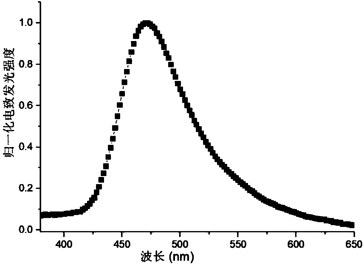
[0058] Such as figure 1 As shown, the hole injection layer 3 in the device structure is PEDOT:PSS, the hole transport layer 4 is TAPC, the host material in the blue light-emitting layer 5 is, and the guest material is a blue light-emitting material emitterB with thermally activated delayed fluorescence characteristics. The electron donor is an acridine group, the electron acceptor is a diphenyl sulfone group, the doping mass ratio is guest material: host material=50%, the material used for the electron transport layer 6 is DPEPO, and the cathode layer is Mg:Ag alloy, The ratio is 10:1. The entire device structure is described as:
[0059] Glass substrate / ITO / PEDOT:PSS(40nm) / TAPC(60nm) / MCP:0.1%emitterB(20nm) / DPEPO(40nm) / Mg:Ag(10:1,100nm)
[0060] The preparation steps of the device are similar to those in Example 1.
PUM
| Property | Measurement | Unit |
|---|---|---|
| Sheet resistance | aaaaa | aaaaa |
| Film thickness | aaaaa | aaaaa |
Abstract
Description
Claims
Application Information