Supercharge Your Innovation With Domain-Expert AI Agents!

A method to realize enhanced III-V HEMT devices using all-solid-state batteries

A III-VHEMT, all-solid-state battery technology, applied in semiconductor/solid-state device manufacturing, semiconductor/solid-state device components, electric solid-state devices, etc., can solve problems such as depletion, difficulty in precise control, and reliability, and achieve high Performance, Effect of High Electron Mobility

Active Publication Date: 2021-01-29
HANGZHOU DIANZI UNIV
View PDF4 Cites 0 Cited by
  • Summary
  • Abstract
  • Description
  • Claims
  • Application Information

AI Technical Summary

Problems solved by technology

This technology takes advantage of the small size of F ions to inject negatively charged F ions into the barrier layer under the gate, resulting in the depletion of 2DEG.
[0003] The first technique is difficult to obtain accurate etching depth, and it is easy to cause damage to the channel
The second technique, the growth of P-type materials, significantly increases the cost of material growth
The third technology is difficult to control accurately, and there are hidden dangers in reliability

Method used


Image

  • A method to realize enhanced III-V HEMT devices using all-solid-state batteries
  • A method to realize enhanced III-V HEMT devices using all-solid-state batteries
  • A method to realize enhanced III-V HEMT devices using all-solid-state batteries

Examples


Embodiment 1

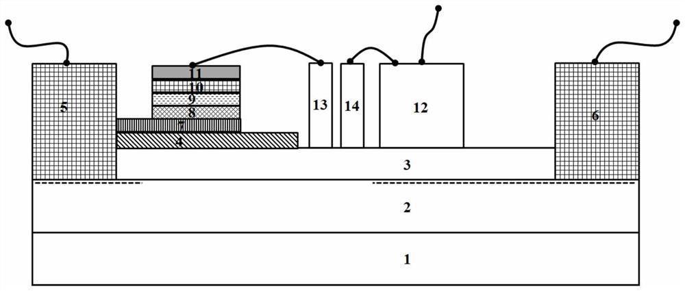
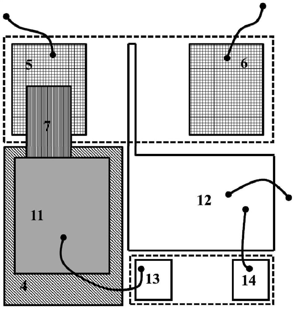
[0059] refer to figure 1 , the basic HEMT of the device is AlGaN / GaN HEMT. Its isolation insulating layer is Si 3 N 4 , with a thickness of 100-200nm, prepared by LPCVD process.

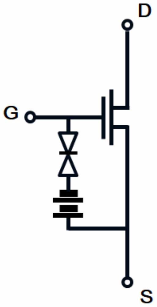
[0060] Si by electron beam evaporation 3 N 4 A 150nm Ni metal layer is sputtered on the top, and then a lithium phosphate ceramic target is used as a sputtering source, and a 500-2000nm LiPON thin film is prepared on the Ni metal by radio frequency magnetron sputtering. Second, 250nm LiCoO was sputtered on the LiPON film 2 film. After that in LiCoO 2 Evaporate Ti / platinum Pt metal with a thickness of 10 / 200nm on the film, and finally make a gate electrode and a diode pair on the surface of AlGaN. The anode metal of the diode is Ni / Au (50 / 200nm), and the turn-on voltage of the single-stage diode is about 1~ 1.5V, and finally the basic HEMT device is electrically connected to the all-solid-state battery and the diode pair through wire bonding technology.

[0061] Further, the area occupied by ...

Embodiment 2

[0063] The base HEMT for this device is an AlN / GaN HEMT. Its isolation insulating layer is Si 3 N 4 , with a thickness of 300nm, prepared by LPCVD process.

[0064] Using radio frequency magnetron sputtering method on 300nm thick Si 3 N 4 250nm Ti metal was deposited on it, followed by LiMn 2 o 4 The target is a sputtering source, and 800nm ​​LiMn is prepared on Ti metal by radio frequency magnetron sputtering. 2 o 4 film, then with Li 3 PO 4 As the sputtering source, in LiMn 2 o 4 A 500nm LiPON film is prepared on the film as an all-solid electrolyte, followed by a 450nm ZnO film on the LiPON film, then a 250nm Ti metal on the ZnO film layer, and finally a gate electrode and a diode pair on the AlN surface, the anode metal of the diode Using Ni / Au (50 / 200nm), the turn-on voltage of the single-stage diode is about 1-1.5V. Finally, the basic HEMT device, the all-solid-state battery and the diode pair are electrically connected by wire bonding technology.

[0065] Th...


PUM

PropertyMeasurementUnit
radiusaaaaaaaaaa

Abstract

The invention discloses a method for realizing an enhanced III-V HEMT device by using an all-solid-state battery. A second semiconductor layer and a first semiconductor layer are sequentially formed on a substrate, and a second semiconductor layer and a first semiconductor layer are formed between the second semiconductor layer and the first semiconductor layer. A heterostructure is formed between them; the source electrode and the drain electrode are electrically connected through the two-dimensional electron gas formed in the heterostructure; the gate electrode is used to control the conduction or disconnection of the two-dimensional electron gas in the heterostructure; and It includes an all-solid-state battery arranged between the source electrode and the gate electrode, and the all-solid-state battery is composed of at least one set of battery cells connected in series or series-parallel to deplete the two-dimensional electron gas in the corresponding region of the heterostructure. The invention can effectively realize the enhanced working mode. In addition, the all-solid-state battery is compatible with the micro-nano processing technology, and can be completed once in the process of the device. Meanwhile, the threshold voltage of the device can be changed by the number of cells of the solid-state battery in series.

Description

technical field [0001] The invention relates to the field of microelectronic devices, in particular to an enhanced III-V HEMT (High Electron Mobility Transistor, high electron mobility transistor) device obtained by introducing a combination structure of an all-solid-state battery and a diode pair (all-solid-state battery combination structure). Background technique [0002] With the advancement of technology, people have higher and higher requirements for the cut-off frequency, power density, switching loss and other indicators of microelectronic devices. All these goals have attracted people to focus on III-V HEMT devices. Taking the most typical AlGaN / GaN device as an example, due to its excellent performance, it has important applications in 5G communication, phased array radar, photovoltaic power generation, electric vehicles and other fields. As a typical III-V device, due to the symmetry of the crystal structure, there are strong spontaneous polarization and piezoelec...

Claims


Application Information

Patent Timeline
Patent Type & Authority Patents(China)
IPC IPC(8): H01L21/335H01L29/778H01L23/58
CPCH01L23/58H01L29/66462H01L29/7786
Inventor 董志华张佩佩张辉程知群李仕琦刘国华蒋俊杰
Owner HANGZHOU DIANZI UNIV
Features
  • R&D
  • Intellectual Property
  • Life Sciences
  • Materials
  • Tech Scout
  • Unparalleled Data Quality
  • Higher Quality Content
  • 60% Fewer Hallucinations
Learn More