Two-color full-fluorescent white-light OLED device

A full fluorescent, blue fluorescent technology, applied in the field of organic optoelectronic devices, can solve the problems that affect the life of the device, affect the promotion of white OLED industrialization, increase the driving voltage of the device, and achieve the effect of simple device structure

Active Publication Date: 2018-09-21
SHANXI DATONG UNIV
View PDF4 Cites 7 Cited by
  • Summary
  • Abstract
  • Description
  • Claims
  • Application Information

AI Technical Summary

Problems solved by technology

The increase of the heterojunction interface makes a large number of carriers gather at the interface, which not only increases the driving voltage of the

Method used


Image

  • Two-color full-fluorescent white-light OLED device
  • Two-color full-fluorescent white-light OLED device
  • Two-color full-fluorescent white-light OLED device

Examples


preparation example Construction

[0049] During the preparation process of the device, the evaporation rate of the material and the thickness of the organic and inorganic film layers are monitored and controlled by a quartz crystal frequency meter connected outside the vacuum chamber. Among them, organic materials, MoO 3 The evaporation rates of LiF, LiF, and Al are about 1Å / s, 0.3Å / s, 0.1Å / s, and 3Å / s, respectively. The overlapping part of the ITO glass and the aluminum cathode is used as the effective light-emitting layer of the device, and the effective light-emitting area is 3mm×3mm.

[0050] The performance test method of the OLED device involved in the embodiment of the present invention is as follows.

[0051] Take out the prepared white OLED device from the vacuum cavity, and measure the current density, luminance, current efficiency and power efficiency of the device by using the computer integrated control ST-900M photometer and Keithley 2400 digital source meter; use computer integrated control Th...

Embodiment 1

[0054] According to the above specific implementation manner, by changing the thickness of the blue fluorescent light-emitting layer spaced between the hole transport layer and the yellow excimer-doped layer, the first group of two-color all-fluorescent white light OLED devices are prepared.

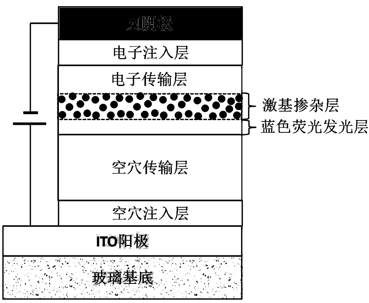
[0055] The specific device structure is: ITO / MoO 3 (3 nm) / TAPC (40 nm) / Bepp 2 (x nm) / Bepp 2 :m-MTDATA (1:1 10 nm) / Bepp 2 (40 nm) / LiF (1 nm) / Al (100 nm).

[0056] In the above white OLED device, ITO is the anode, and the 3nm thick MoO 3 The thin layer is the hole injection layer, the 40nm thick TAPC layer is the hole transport layer, and the x nm thick Bepp 2 The layer is a blue fluorescent light-emitting layer, its x=5, 7, 9 nm, 10nm thick Bepp 2 :m-MTDATA (1:1) layer is a yellow excimer doped layer, 40nm thick Bepp 2 The LiF layer is the electron transport layer, the 1nm thick LiF layer is the electron injection layer, and the 100nm thick Al film is the cathode.

[0057] ...

Embodiment 2

[0062] In order to further verify the feasibility of the device structure of the two-color all-fluorescent white light OLED of the present invention, taking the device W2 which obtained the optimal device performance in Example 1 as a reference, changing the doping concentrations of the donor and the acceptor in the excimate-doped layer, prepared a Devices W4 and W5.

[0063] The specific device structure is: ITO / MoO 3 (3 nm) / TAPC (40 nm) / Bepp 2 (7 nm) / Bepp 2 :m-MTDATA (2:1 or 1:2 10 nm) / Bepp 2 (40 nm) / LiF (1 nm) / Al (100 nm).

[0064] Among them, the device corresponding to the acceptor and donor doping concentration of 2:1 in the excimer doped layer is named W4, and the device corresponding to the doping concentration of 1:2 is named W5.

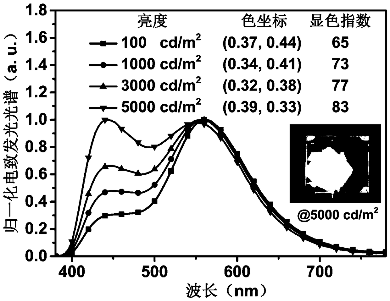
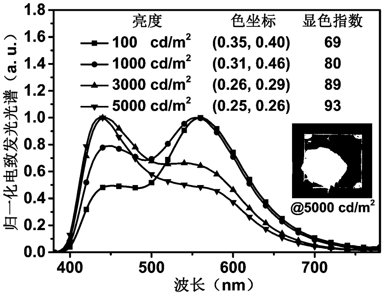
[0065] Figure 5 with Image 6 The normalized electroluminescence spectra of devices W4 and W5 at different brightnesses are given, respectively. Compared with device W2, the high or low doping concentration of donor and accep...


PUM

PropertyMeasurementUnit
Thicknessaaaaaaaaaa
Thicknessaaaaaaaaaa

Abstract

The invention discloses a two-color full-fluorescent white-light OLED device. A light-emitting layer of the device is formed by a blue fluorescent light-emitting layer and an excimer doping layer. Theblue fluorescent light-emitting layer is close to the side of a hole transport layer, and the light-emitting material is same with the electron transfer layer material; and the excimer doping layer is close to the side of an electron transfer layer, and is formed by doping an excimer donor material in an excimer receptor material, which is same with the electron transfer layer material. The excimer doping layer can realize yellow light emission, which is complementary to blue light emission of the blue fluorescent light-emitting layer to form white light, thereby realizing double-color whitelight emission. In the OLED device, the blue fluorescent light-emitting layer material and the excimer receptor material and the electron transfer layer material are same, so that the device is simplein structure, easy in the preparation process and low in cost.

Description

technical field [0001] The invention belongs to the technical field of organic optoelectronic devices, and relates to organic electroluminescence devices, in particular to an all-fluorescence white light organic light emitting diode. Background technique [0002] Organic light-emitting diodes (OLEDs), because of their unique advantages, such as fast response speed, high color quality, light and thin, low manufacturing cost, flexible and transparent preparation, etc. Become the next generation of new display and lighting technology. [0003] White light OLED is the main application product in the field of lighting. The currently prepared white light OLEDs mainly have three device structures: single emitting layer, multi-emitting layer and laminated emitting layer. [0004] Single-emitting layer white light OLEDs are usually obtained by simultaneously doping two or three complementary light-emitting materials into the same host material, or doping a blue-emitting host materi...

Claims


Application Information

Patent Timeline
IPC IPC(8): H01L51/50B82Y40/00
CPCB82Y40/00H10K50/12H10K50/13
Inventor 高志翔苗艳勤冯子龙屈文山李建刚李榜全石云龙
Owner SHANXI DATONG UNIV
Why Eureka
Try Eureka