A solid welding process for heat dissipation chips

A welding process and chip body technology, applied in welding equipment, electrical solid devices, manufacturing tools, etc., can solve the problems of high void rate and a large number of voids in chip bonding, reduce void rate, eliminate voids, and improve inherent reliability Effect

Active Publication Date: 2020-06-26
西安君信电子科技有限责任公司
View PDF6 Cites 0 Cited by
  • Summary
  • Abstract
  • Description
  • Claims
  • Application Information

AI Technical Summary

Problems solved by technology

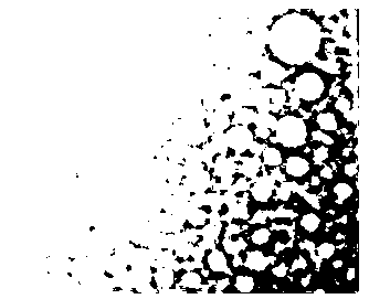
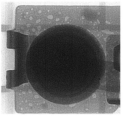
[0005] In order to solve the problem of high void rate in chip bonding in the prior art, the present invention provides a solid soldering process, which solves the problem of easy soldering in the adhesive layer in the traditional process by adopting hot isostatic pressing technology. The problem of creating a large number of voids

Method used


Image

  • A solid welding process for heat dissipation chips
  • A solid welding process for heat dissipation chips
  • A solid welding process for heat dissipation chips

Examples


Embodiment 1

[0040] Refer to attached Image 6 Shown, the technology in the present embodiment is as follows:

[0041] The first step is to select the chip body 1 and the first heat dissipation device that matches the chip body 1; there can be one or more first heat dissipation devices. In this embodiment, there is one first heat dissipation device. When it is placed, It can be arranged on any side of the chip body 1 .

[0042] The second step is to install the heat dissipation chip; specifically, place the chip body 1 and the first heat dissipation device in the sealed cabin of the hot isostatic press at the same time, and perform vacuuming operation on the sealed cabin; Injecting an inert gas, using a hot isostatic pressing process to connect the chip body 1 to the first heat sink in a solid phase;

[0043] In the hot isostatic pressing process, the heating temperature is 0.3-0.8 times the melting point temperature of the first heat sink.

[0044]In this embodiment, the heating temper...

Embodiment 2

[0051] Refer to attached Figure 6-7 As shown, the present invention discloses a solid welding process for a heat dissipation chip. In this embodiment, the chip body 1 is provided with first heat dissipation devices above and below, and the first heat dissipation devices are respectively a first heat dissipation plate 4 and a second heat dissipation plate. Radiating plate 5.

[0052] Specifically include the following steps:

[0053] The first step, the formation of the first heat dissipation device: the chip body 1, the first metal sheet 2, the first heat dissipation plate 4 and the second heat dissipation plate 5, the finished chip is arranged according to the first heat dissipation plate 4, the first metal sheet from top to bottom 2. The chip body 1 , the second metal sheet 3 and the second heat dissipation plate 5 are stacked in order to form a chip with the first heat dissipation device.

[0054] In this embodiment, a metal sheet is disposed between the first heat dissi...

Embodiment 3

[0064] In this embodiment, a solid welding process for a heat dissipation chip, in this embodiment, there are four heat dissipation devices, the first heat dissipation plate 4, the second heat dissipation plate 5, the copper electrode sheet 6 and the copper base 7, and its layers are arranged on The upper and lower surfaces of the chip body 1 are provided with two types of heat dissipation devices on the upper surface and the lower surface of the chip body 1 respectively in this embodiment in order to improve the heat dissipation effect.

[0065] This embodiment specifically includes the following processes:

[0066] The first step, pretreatment of the chip body 1: performing impurity removal on the chip body 1;

[0067] Specifically, the chip body 1 is thinned to 270um-360um, the upper and lower surfaces of the chip body 1 are respectively polished, and at the same time, the upper and lower surfaces of the chip are bombarded by a plasma machine for 2 minutes to complete the p...


PUM


Abstract

The invention relates to a solid welding process of a cooling chip. The solid welding process of the cooling chip comprises the following steps that (1) a first cooling device matched with a chip bodyis selected; and (2) the cooling chip is assembled, specifically, the chip body and the first cooling device are put in a sealing bin of a hot isostatic press at the same time, the sealing bin is vacuumized, inert gas is injected into the sealing bin after vacuumizing, the chip body and the first cooling device are connected in a solid state mode through a hot isostatic pressure process, and in the hot isostatic pressure process, the heating temperature is 0.3-0.8 time of the melting temperature of the first cooling device. The cooling chip prepared by the solid welding process has good heatdissipation performance, low voidage and high overall use performance.

Description

technical field [0001] The invention belongs to the technical field of chip packaging and processing, and in particular relates to a solid welding process for a heat dissipation chip. Background technique [0002] Power devices are widely used in the fields of electronics, electric power, and high-speed rail. They usually work under high voltage and high current conditions. When they work, their self-heating and loss are serious, and the application environment is harsh. Therefore, power devices are prone to failure and cause certain economic losses. and accidents. Among the failures of power devices, a small part is caused by use problems. Most of the failures are caused by the process and quality problems of the power device itself, and the most common process and quality problem of power devices is the problem of chip bonding voids. Brazing and eutectic welding (such as tin-lead solder, gold Antimony alloy sheet, tin-silver-copper, tin-lead-silver, conductive glue and o...

Claims


Application Information

Patent Timeline
Patent Type & Authority Patents(China)
IPC IPC(8): H01L23/367H05K3/34B23K20/02
CPCB23K20/002B23K20/021B23K20/023
Inventor 王宏全
Owner 西安君信电子科技有限责任公司
Why Eureka
Try Eureka